Abstract
FPGA based Quasi Z-Source Cascaded Multilevel Inverter (Quasi Zs-CMLI) using multicarrier PluseWidth Modulation (PWM) techniques are presented in this paper. Multicarrier based PWM techniques have been proposed for seven level Quasi Zs-CMLI and implemented using Field Programmable Gate Array (FPGA). For generating gating pulses to the inverter switches, Phase Disposition (PD), Inverted Phase Disposition (IPD), Phase Opposition Disposition (POD) and Alternative Phase Opposition Disposition (APOD) techniques are programmed on FPGA. In the proposed system, three solar PV emulator modules are used. These are acting as input source to the inverter. Finally, THD comparison made between different carrier based modulation with shoot through and non-shoot through the states. The proposed quasi Zs-CMLI and PWM techniques are verified through MATLAB/Simulink. For confirmation of simulation results, A laboratory prototype model have been implemented using FPGA. The capture hardware results are matched with simulation results.
1. Introduction
In recent years, Multilevel inverters(MLIs) have drawn tremendous interest in the area of high voltage and high-power applications along with renewable energy sources such as wind energy systems, Photovoltaic (PV) systems, Fuel cell etc. MLIs having numerous features such as low distortion output waveform, reduced voltage stress, reduced EMI, operate with lower switching frequency and higher efficiency [1]. MLIs are classified into three types, they are (i) Diode clamped MLIs (ii) Flying capacitor MLIs (iii) Cascaded MLIs. Among the MLIs, the cascaded MLI structure is well suited for a PV system, but it has some own drawbacks like three stage power conversion, lower efficiency and short circuit problem. To overcome the drawbacks of conventional inverter, Z-source inverter have been presented in this paper [2]. The Zs-CMLI uses the LC impedance network to connect a DC voltage source to the inverter [3, 4]. The Z-source inverter translate the zero state of traditional inverter into a shoot-through (short circuit) states, thereby achieving the buck/boost of the input DC source. The Z-source inverter structure has several advantages as compared to traditional inverter, including lower costs, single stage conversion and more reliable. Even though, Z-source inverters suffer from the drawback of discontinuous input current that lead to very high harmonics. So that the impedance network is modified to form the quasi Z-source inverter that has continuous input current with reduction in voltage rating of impedance network [4-8]. The Quasi Zs-CMLIs are mainly used in the photovoltaic power generation system that has advantage of balanced DC-link voltage control, distributed maximum power tracking, modular structure and reduced AC side filter requirements. These features cannot be realized in traditional CMI. There are several multicarrier based PWM techniques used to control the output voltage of traditional MLI. The multicarrier PWM can be implemented with less complexity, offers better performance in all the operating conditions and also allow the over modulation region [7-10]. The contribution of this papers: Six different carrier based PWM techniques such as triangular, sawtooth, unipolar, sine(regular), stepped wave and staircase with four modulation schemes (PD, IPD, POD and APOD) are implemented for Quasi Zs-CMLI. In this work, the emulator has been used as input to the Quasi Zs-CMLI. The performance of multicarrier techniques are analysed in terms of THD % profile with a different modulation index and effect of the carrier wave on the shoot-through state also analysed. The prototype model of the proposed system has been implemented using FGPA and tested with different modulation schemes for the seven level quasi under ST and NST conditions.
2. Quasi Z-source inverter
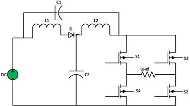
The single phase quasi Z-source inverter circuit is shown Fig. 1(a). This inverter consists of quasi Z-source along with a normal H bridge inverter. Quasi Z-source consists of two inductors ( and – 2 mH), two capacitors ( and – 3300 mF) and diode. Normal H-bridge inverter consists of four MOSFETs (, , and ). The Quasi Zs-CMLI operates at two modes of operation, namely: Non-Shoot Through(NST) mode and Shoot-Through (ST) mode.
Fig. 1Circuit diagram, 1: a) single stage quasi Z-source b) quasi at ST mode 1, c) quasi at NST mode
a)
b)
c)
The equivalent circuit of ST and NST modes are shown in Fig. 1(b) and 1(c) respectively. In NST mode, Quasi Zs-inverter operate as a normal traditional inverter and its operate at active state. The capacitor is charged to the input voltage and charged to voltage across the , the voltage across the inductor (, , capacitor, and are expressed as:
Assume is total switching period, which is an inversion of switching frequency , is the shoot-through period and is non-shoot through the period.so that . Fig. 1(a)-(c). shows equivalent circuits of single stage quasi, ST and NST conditions. In ST mode, Quasi Zs-inverter operates as a buck/boost converter and it operates at zero state. The diode is reverse biased due to capacitor voltage exceeds the input voltage. Now, is discharged through and input current continue to flow through and . After ST mode, the energy transferred to the inductance is added to the normal state and hereby boosted voltage is obtained. The average inductor voltage and over the switching cycle is zero. The average capacitor voltage is expressed as:
The DC-link voltage can be derived by substituting Eqs. (3) and (4) in Eq. (2):
where, is the boost factor of Quasi Zs-CMLI. The Quasi Zs-CMLI are highly suited for PV systems, individual PV emulators can be connected at each H-bridge input. Each H-bridge inverter produce three level output, namely , 0 and . The output load voltage has a number of levels equal to 2 1 where n is the number of input DC sources.
3. Seven level quasi Z-source cascaded multilevel inverter
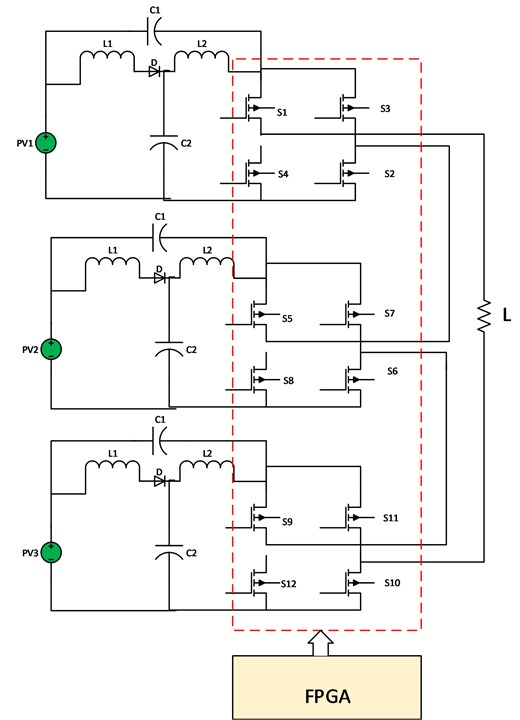
Fig. 2. Shows the power circuit diagram of proposed FPGA based quasi Z-source CMLI topology where each H-bridge has LC impedance and impedance network fed from the individual PV emulators.
Table 1Switching states of seven-level quasi Z-source Inverter
Voltage level | Output voltage | State | On switches |
Level 1 | +3VDC | Active state | S1, S2, S5, S6, S9, S10 |
Level 2 | +2VDC | Active state | S1, S2, S5, S6, S9, S11 |
Level 3 | +1VDC | Active state | S1, S2, S5, S7, S9, S11 |
Level 4 | 0 | Zero state | S4, S2, S8, S7, S12, S10 |
Level 4 | 0 | Shoot-through state | S1 To S12 |
Level 5 | –VDC | Active state | S3, S4, S6, S8, S10, S12 |
Level 6 | –2VDC | Active state | S3, S4, S7, S8, S10, S12 |
Level 7 | –3VDC | Active state | S3, S4, S7, S8, S11, S12 |
The switching states of Quasi Zs-CMLI are shown in the Table 1. In each active state, six switches have in ‘ON state’ and other switches been in ‘OFF position’. During zero state, all the switches are turned to ‘ON state’ for the boost operation of quasi network. The switching states of seven level Quasi Zs-CMLI shown in the Table 1.
4. Multicarrier based sine pulse width modulation techniques
In this paper, six multicarrier based SPWM techniques combined to shoot-through state and simple boost technique developed for Quasi-CMI as follows: Triangular (TMC), Saw Tooth (STMC), Unipolar Sine (UPMC), Sine (Regular) (SMC), Stepped (SPMC) and Staircase (SCMC). Multicarrier PWM techniques entail the natural sampling of a single modulating or reference waveform typically being sinusoidal same as that of output frequency of the inversion system, through several carrier signals.
Fig. 2FPGA-based seven level quasi Z-source CML
There are different scheme of switching techniques have been proposed for controlling of multilevel inverters. There are two types of carrier based PWM are i) Phase shifted carrier PWM and Carrier disposition PWM. Further, Carrier disposition PWM classified into Alternate Phase opposition disposition (APOD), Phase Opposition Disposition (POD) and Inverse Phase Disposition (IPD). In the PD switching methods, (M-1) the carrier signals have same phase and frequency. APOD Switching methods is very similar to PD but only difference is each carrier signals phase shifted by 180° from the adjust carrier. In this control technique, most of the harmonics are appeared at around the carrier frequency. In the phase opposition methods, (M-1) carrier signals are required to generate gating pulses for the N level inverter and upper half of the two signals are in same phase and lower half will be 180° out of phase with upper half. In the IPD PWM approach the level shifted carrier signal are 180° out of phase when compared to the PD. These carrier signals are compared with a sinusoidal modulating wave. The reference or modulation waveform has peak amplitude and frequency , and it is centered in the middle of the carrier set. If the reference is greater than the carrier signal, then the active device corresponding to that carrier is switched ON, and if the reference is less than the carrier signal, then the active device corresponding to that carrier is switched OFF. The carrier frequency defines the switching frequency of the converter. Modulation index of multilevel inverters is defined as:
where, and are the amplitude of the reference and the carrier signal respectively.
5. Simulation results
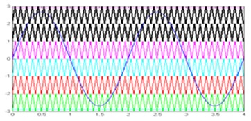
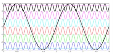
The seven level quasi Z-source inverter has been simulated using MATLAB/SIMULINK. The PD, IPD, POD, and APOD modulation schemes are used for the six multicarrier SPWM techniques. The operating frequency of the Quasi Zs-CMLI is 5 kHz where as 1 kHz to 10 kHz switching frequency used in the existing literature. The inverter gives poor THD performance at lower operating frequency while inverter offers good performance at higher frequencies (10 kHz). However, higher frequency of operation will lead to higher switching losses. Hence, 5 kHz switching frequency has been chosen in this proposed work. The THD performances of the proposed system have been evaluated and compared with all modulation techniques. These modulation strategies are implemented and illustrated from Figs. 3(a)-3(f).
Fig. 3Simulation waveforms for multicarrier SPWM techniques
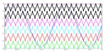
a) TMC PD technique
b) STMC APOD technique
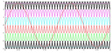
c) UPMC POD techniques
d) SMC PD techniques
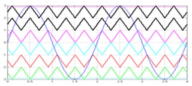
e) SPMC PD techniques
f) SCMC POD techniques
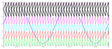
Fig. 4Switching pulse with shoot through ratio D0= 10 % and modulation index Ma= 0.9
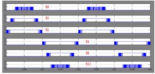
Fig. 5S1: Switching pulse for S1 switch, ST: Shoot-through pulse, ZS: Zero state, S1+ST: S1 pulses combined with ST wave
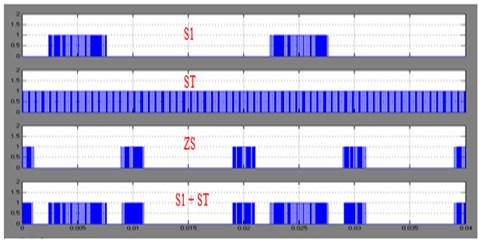
Fig. 6Switching pulse with shoot through ratio D0= 90 % and modulation index Ma= 0.9
The switching pulses are generated from simulation and shown in Figs. 4-6. The output voltage and harmonic spectrum of proposed system are obtained for fundamental frequency with different duty ratio. The MATLAB simulation has been carried for duty ratio of 10 % and Modulation index 0.9 and duty ratio of 90 % and Modulation index 0.9. Here, only presents, duty ratio of 90 % and Modulation index 0.9. Table 2 shows the fundamental load voltage and load voltage THD % for the six carriers with shoot through ratio 90 % and modulation index 0.9. The Quasi Zs-CMI operate as a boost converter. The boost factor is set as 2. The seven level output voltage obtained are approximately , ±90 V, ±180 V and ±270 V.
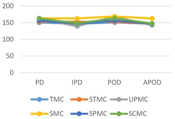
From Table 1, it is observed that, the TMC POD and TMC PD methods provide almost equal to the calculated value. However, TMC APOD PWM gives minimum (i.e. boost factor compared to the other modulation within TMC PWM methods). In all available literature, the boost factor is derived only for the triangular carrier waveform. This paper analyses the effect of another carrier waveform. From the simulation results, it is inferred that, stepped carrier (PD, APOD modulation) and staircase carrier (PD, APOD modulation) achieved the maximum boost. In terms of % THD, SMC PWM gives a minimal voltage and current THD of 9.17 % and 8.96 % compared to the other methods. The load voltage, load current waveform (RL load- 20 Ohms, 1 mH) and corresponding harmonic spectrum are shown in the Figs. 7 to 10 respectively. Figs. 11 and 12 show the output load voltage value against % THD respectively. The fundamental load current and load current THD % are given in the Table 3.
Table 2Output load voltage %THD for Seven-Level Quasi-CMI with shoot-through ratio = 90 %
Load voltage %THD | ||||||||||||
Shoot-through ratio = 90 % | ||||||||||||
SPWM modulation | TMC | STMC | UPMC | SMC | SPMC | SCMC | ||||||
Volt V) | THD (%) | Volt V) | THD (%) | Volt V) | THD (%) | Volt V) | THD (%) | Volt V) | THD (%) | Volt V) | THD (%) | |
PD | 266.00 | 12.19 | 266.00 | 12.61 | 231.1 | 10.27 | 230.30 | 9.52 | 320.20 | 17.85 | 312.80 | 18.53 |
IPD | 252.60 | 12.64 | 266.80 | 10.46 | 207.00 | 13.78 | 227.70 | 9.17 | 254.10 | 13.80 | 279.80 | 17.27 |
POD | 273.00 | 13.44 | 279.40 | 11.44 | 303.00 | 14.36 | 229.10 | 9.31 | 320.20 | 17.85 | 312.80 | 18.53 |
APOD | 245.00 | 11.86 | 234.00 | 09.57 | 209.10 | 15.91 | 228.10 | 9.42 | 254.10 | 13.34 | 279.70 | 17.35 |
Table 3Output load current %THD for Seven-Level Quasi-CMI with shoot-through ratio = 90 %
Load current % THD | ||||||||||||
Shoot-through ratio = 90 % | ||||||||||||
SPWM modulation | TMC | STMC | UPMC | SMC | SPMC | SCMC | ||||||
Amp (A) | THD (%) | Amp (A) | THD (%) | Amp (A) | THD (%) | Amp (A) | THD (%) | Amp (A) | THD (%) | Amp (A) | THD (%) | |
PD | 13.30 | 11.98 | 14.00 | 12.76 | 13.09 | 10.06 | 13.00 | 9.30 | 16.01 | 14.75 | 15.64 | 15.64 |
IPD | 12.63 | 12.46 | 13.34 | 10.29 | 10.36 | 13.59 | 12.76 | 8.96 | 12.7 | 11.93 | 13.99 | 14.41 |
POD | 13.65 | 13.24 | 13.97 | 11.30 | 7.094 | 7.49 | 12.9 | 9.09 | 16.01 | 14.75 | 15.64 | 15.64 |
APOD | 12.22 | 11.66 | 11.69 | 9.67 | 10.45 | 15.72 | 12.8 | 9.6 | 12.71 | 11.49 | 13.98 | 14.50 |
Fig. 7Load voltage
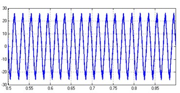
Fig. 8Load current
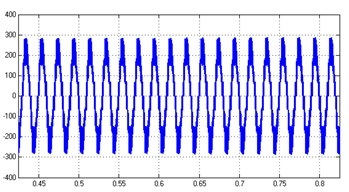
Fig. 9Voltage harmonics spectrum
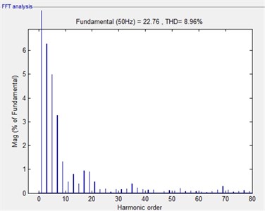
Fig. 10Current harmonics spectrum
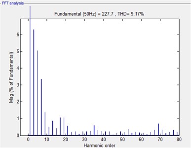
Fig. 11Load voltage THD % shoot through ratio D0= 90 % and Modulation index Ma= 0.9
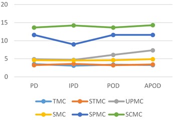
Fig. 12Load voltage value shoot through ratio D0= 90 % and Modulation index Ma= 0.9
6. Hardware results
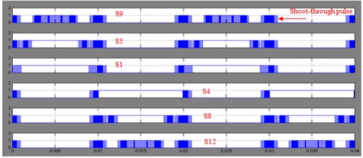
The Quasi Zs-CMLI using multicarrier PWM techniques has been implemented using the FPGA based prototype model. It consists of three quasi Z-source network, PV Emulator, three full H-bridge, load and FPGA-Spartan-6 controller. The switching pulses generated from FPGA are shown in Figs. 13-15.
Fig. 13Switching Pulse for S1, S2, S3 and S4 with shoot through ratio D0= 90 % and modulation index Ma= 0.9
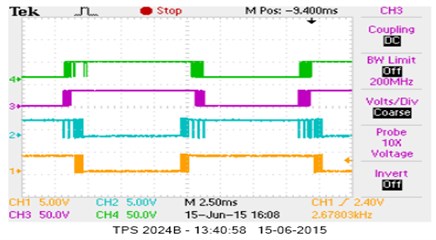
Fig. 14Switching pulse for S5, S6, S7 and S8 with shoot through ratio D0= 90 % and modulation index Ma= 0.9
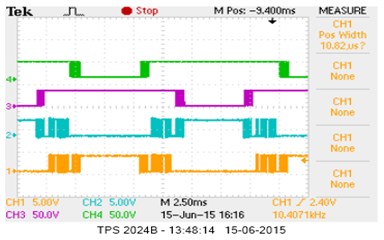
Fig. 15Switching pulse for S9, S10, S11 and S12 with shoot through ratio D0= 90 % and modulation index Ma= 0.9
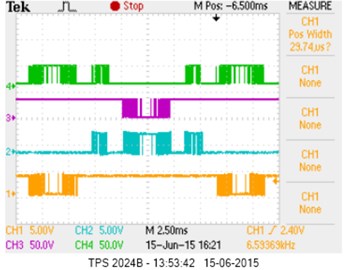
The prototype model of the proposed system has been designed using IRF250N MOSFETs and IN5408 diodes. In this hardware setup, three Solar PV Emulators are used which acting as input DC source (20V) for the Quasi Zs-CMLI. The impedance network consists of 4700 μf capacitors and 2 mH inductors. The SPWM switching signals are generated with help of Spartan-6 (XC6SLX9) FPGA controller. The generated switching signals are interfaced to the inverter power switches through driver TLP250. The switching frequency is 5 KHz. The hardware results are captured using Fluke power spectrum analyser and measured gating pulses are shown in Figs. 13, 14 and 15 respectively. The experimental results of seven-level output voltage and current waveform are shown in Figs. 16 and 17for 10 % and 90 %, respectivelyThe experimental voltage and current harmonics are shown in the Figs. 18 and 19. The THD % obtained from experimental method is 4 % at 10 % for TMC SPWM techniques which is below the IEEE standards. Table 4 shows the comparison of simulation and hardware results. From Table 4, it is observed that simulation results are good agreement with hardware results.
Fig. 16Load voltage and current for shoot-through ratio D0= 10 % and modulation index Ma= 0.9 (CH 2:20V/DIV, 5 ms/DIV
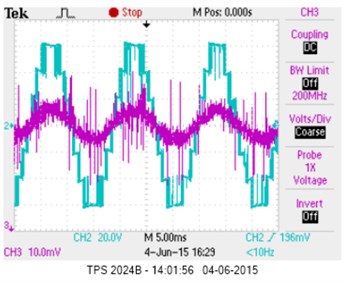
Fig. 17Load voltage and current for shoot-through ratio D0= 90 % and modulation index Ma= 0.9 (CH 2:50V/DIV, 10 ms/DIV)
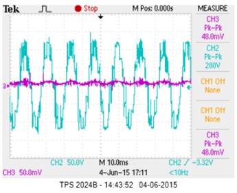
Fig. 18Load voltage harmonic spectrum at D0= 10%
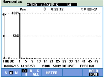
Fig. 19Load voltage harmonic spectrum at D0= 90 %
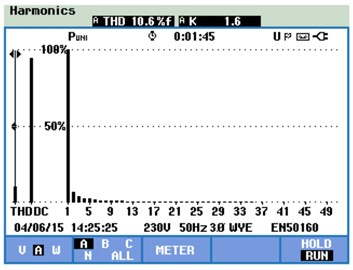
Table 4Comparison of simulation and hardware results
Input voltage (V) | Boost factor | Output voltage (V) 10 % | Output voltage (V) 90 % | Output voltage THD % | |
10 % | 90 % | ||||
Simulation 20 V | 2 | 60 V | 140 V | 2.89 | 12.01 |
Experiment 20 V | 2 | 60 V | 140 V | 4.00 | 10.60 |
7. Conclusions
In this work, multicarrier based SPWM techniques with different duty ratio has been implemented using FPGA for seven-level Quasi Zs-CMLI. The THD profile and voltage boost capability of the proposed system has been analysed and compared with duty ratio of 10 % and 90 % respectively. From the analysis, it is observed that phase opposition disposition (POD) Sine-Regular multicarrier technique offers the minimal voltage THD of 4 % for shoot through duty ratio of 10 % over other modulation and PWM techniques. The simulation results of proposed seven-level Quasi Zs-CMLI has been validated through FPGA controller based prototype model. The boosted voltage and percentage THD profile obtained from the prototype model are in good agreement with the simulation results.
References
-
Venkatesan Mani, Rajeswari Ramachandran, Devarajan Nanjundappan Implementation of a modified SVPWM-based three-phase inverter with reduced switches using a single DC source for a grid-connected PV system. Turkish Journal of Electrical Engineering and Computer Sciences, Vol. 26, Issue 4, 2016, p. 3023-3035.
-
Peng F. Z. Z-source inverter. IEEE Transactions on Industry Applications, Vol. 39, 2003, p. 504-510.
-
Wei M., Loh P. C., Blaabjerg F. Asymmetrical transformer based embedded Z-source inverter. IET Power Electronics, Vol. 6, Issue 2, 2013, p. 261-269.
-
Liqiang Yang, Dongyuan Qiu, Bo Zhang High-performance quasi Z-source inverter with low capacitor voltage stress and small inductance. IET Power Electronics, Vol. 8, Issue 6, 2015, p. 1061-1067.
-
Siwakoti Y. P., Blaabjerg F., Loh P. C. High voltage boost quasi Z-source isolated DC/DC converter. IET Power Electronics, Vol. 7, Issue 9, 2014, p. 2387-2395.
-
Yushan Liu, Baoming Ge, Abu Rub H. Phase shifted pulse width amplitude modulation for quasi Z-source cascaded multilevel inverter based photo voltaic system. IET Power Electronics, Vol. 7, Issue 6, 2014, p. 1444-1456.
-
Nguyen M. K., Lim Y. C., Choi J. H. Two switched-inductor quasi Z-source inverters. IET Power Electronics, Vol. 5, Issue 7, 2012, p. 1017-1025.
-
Yushan Liu, Baoming Ge, Abu Rub H. Z-source/quasi z-source inverters: derived networks, modulations, controls, and emerging applications to photovoltaic conversion. IEEE Industrial Electronics Magazine, Vol. 8, Issue 4, 2014, p. 32-44.
-
Yushan Liu, Baoming Ge, Abu Rub H. Modelling and controller design of quasi Z-source cascaded multilevel inverter-based three-phase grid-tie photovoltaic power system. IET Renewable Power Generation, Vol. 8, Issue 8, 2014, p. 925-936.
-
Mcgrath B. P., Holmes D. G. Multicarrier PWM strategies for multilevel inverters. IEEE Transactions on Industrial Electronics, Vol. 40, Issue 4, 2002, p. 858-867.
Cited by
About this article

This project is funded by TEQIP Phase II – Centre of Excellence for Alternative Energy Research in the Department of Electrical Engineering, Government College of Technology, Coimbatore, Tamilnadu, India.
