Abstract
This paper presents comparison of properties of NiSi and Ni(Pd)Si for possible application as interconnect and electrode materials for film bulk acoustic resonators (FBAR) and microelectromechanical systems (MEMS). A number of silicide phases including monosilicide and disilicide phases are found to be formed at various temperatures depending on the composition of the annealed film. The addition of palladium is proved to delay nickel disilicide phase formation which results in a lower sheet resistance at higher temperatures and the possibility to use this material as low resistance interconnect or electrode material rather than pure nickel silicide. At the same time the surface morphology of nickel palladium silicide is found to be more homogeneous, with smaller grain sizes and more uniform alignment of grains in the film, altogether providing the better options for perspective application in FBARs and MEMS, compatible with silicon microelectronics.
1. Introduction
Integration of different technologies into a single module while minimizing fabrication process steps, enhancing functionality of materials and diversifying applications is a key objective in any branch of advanced industry. For example, one of the current trends in technology is to create integrated circuit (IC) compatible microelectromechanical systems (MEMS) and film bulk acoustic resonators (FBAR) [1, 2]. As it is known MEMS have earned popularity due to adding mechanical sensing and actuation to electronics as RF switchers, cantilevers, bridges and membranes, while FBAR are used as RF filters, sensors (among them label-free biosensors), power or noise amplifiers and many more [3, 4, 5]. To obtain flexibility to couple multiple science domains there is a need in materials with high compatibility with silicon microelectronics, on the one hand and the ones that could be fabricated together with the materials used for FBARs and MEMS, on the other hand.
The possibility to use NiSi electrodes for the front-end IC integration with electroacoustic technology is shown recently in [1]. In [6] it is reported on NiSi as a mechanical material for cantilevers and bridges. At the same time NiSi is mainly known as a promising contact material for shallow p-n junctions, CMOS structures [7, 8], Schottky diodes [9], photovoltaic applications [10], due to its superior physical properties of low resistivity, low silicon consumption, low temperature of formation, and etc. [11, 12, 13]. Therefore, at first glance, nickel silicide appears to be the best option for the purpose of IC integration of MEMS and FBAR.
Nevertheless, there are current problems to be overcome. NiSi is known for poor thermal and morphological stability at high temperatures due to phase transformation to high resistivity nickel disilicide phase and film agglomeration [7]. Meanwhile, for common contact and electrode layer for 3-D MEMS a material with low resistivity that is constant in a wide range of temperatures, with smooth interface and uniform stress distribution is required [2]. The use of NiSi in FBAR also requires the synthesis of a smooth silicide layer with a thickness of hundreds of nanometers [1]. The latter is an extreme requirement, which has not been matched before due to an inherent resistivity and roughness degradation with silicide. Moreover, only the requirement of temperature stability of NiSi enables subsequent growth of textured piezoelectric AlN or ZnO films, provided that NiSi has a smooth enough surface [1]. It is noted in [11] that the introduction of alloying elements can substantially affect morphological and formation stability of NiSi compound, which becomes beneficial in a wide temperature process technology.
In this paper we show that using Ni(Pd)Si instead of NiSi is promising to adjust thermal and morphological stability for its becoming much more efficient interconnect and electrode material for IC integration of FBAR and MEMS.
2. Experimental procedure
We have performed a traditional silicidation process sequence comprising metal deposition – heat treatment for silicide formation – removal of excess metal. Silicon wafers with orientation (111), -type, were used as substrates. After a standard RCA cleaning process the wafers were loaded into a high-vacuum dc sputter-deposition chamber. Nickel films with the addition of 10 % of palladium alloy and for comparison pure nickel films were deposited at nominal room temperature of the thickness about 100 nm. In Ni(M) alloy, the addition of 5 to 10 % of metal is considered enough to change the thermal stability of silicide, although the addition of 10 % of alloy metal, for example in case of Pt generally retards the formation of NiSi2 more effectively [7]. The silicidation process was carried out in inert gas ambient in vacuum furnace with the first annealing at 475°C for 30 min to form nickel silicide with a subsequent etching of the unreacted metal. Annealing temperatures for the second annealing were varied from 475 up to 900°C and also for 30 min to study the change in morphology, phase transformation and peculiarities of film agglomeration.
The silicide films were characterized using a four-probe for sheet resistance measurements, Raman spectroscopy for phase formation, and SEM and AFM for morphology analysis. Raman measurements were carried out in a backscattering geometry of on a Jobin Yvon LabRam HR 800 UV micro-Raman system with Andor DU420 CCD detector using a 514.5 nm line of Ar+ laser as an excitation source. For scanning electron microscopy we have used JEOL JSM-6460 SEM. AFM was performed by means of atomic force microscope NANATOP NT-206 at room temperature.
3. Results and discussions
Sheet resistance measurements are carried out not only to study electrical properties but also as a method of express-analysis of phase transformation. The variation of sheet resistance displayed in Fig. 1 shows that NiSi films have low values of the sheet resistance in the temperature range of 475-750°С. In the same range of temperatures the Ni(Pd)Si films have higher values of the sheet resistance, as it is seen from Fig. 1. The higher values of the sheet resistance could be due to the presence of an additional metal (Pd), resulting in an initially higher value of the resistance. It is explained by the fact that at interaction of two types of conductors (metals) a series connection is formed, and therefore the values of the resistance are summed up. As it is seen from Fig. 1, a sharp increase (in 2-3 times) of the sheet resistance is noticed in the result of annealing of NiSi film at temperatures higher than 750°С, which is due to both agglomeration and the transformation of the monosilicide phase to the disilicide phase. For Ni(Pd)Si sample we can conclude that nickel monosilicide phase is stable up to 850°С, as the sheet resistance does not alter much. At 900°C it increases in two times, indicating that the phase transformation process has started or a severe agglomeration has occurred.
Hence, in the extended temperature range it is noticeably better to use Ni(Pd)Si film as its resistance is more stable at higher temperatures, indicating the better utilization of this composite silicide for FBAR and MEMS application.
Raman spectroscopy is a very sensitive tool that is mainly used to study vibrational properties of materials, phase identification, strain state, nucleation site density and grain size. Therefore, Raman spectrum serves as a material fingerprint with each peak in the spectrum corresponding to a unique vibrational mode of the lattice. NiSi belongs to the orthorhombic structure (MnP-type, space group Pnma, D2h16) and is Raman active. Usually in Raman spectra of NiSi not all active optical phonons predicted by group theory analysis are observed as their detection is strongly dependent on film quality and crystallinity, although there are usually very distinct first-order peaks that are phase indicative and are used to analyse the progress in phase transformation by Raman spectroscopy.
Fig. 1The sheet resistance of NiSi and Ni(Pd)Si films vs. temperature
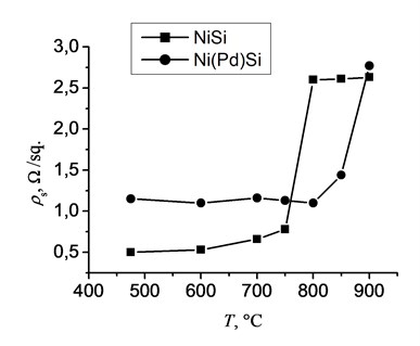
Fig. 2(a), (b) presents the room-temperature micro-Raman spectra of Ni and Ni(Pd) films on Si substrates, annealed at various temperatures. The obtained spectra are in good agreement with previous reports on nickel silicides [14, 15]. At 475-750°C the Raman spectra indicates the formation of NiSi phase. The strongest peak at about 214 cm-1 and the weak peaks at 291, 362, and 398 cm-1 are assigned to Ag modes [14]. The second strongest peak at 196 cm-1 and another weak one at 255 cm-1 belong to B1g and B2g phonon modes, respectively [14]. Negligibility of peaks at 255 and 398 cm-1 could be due to the orientation effects in polycrystalline films. Full transformation to NiSi2 phase occurs at 800°C as the first-order Raman peak at 214 cm-1 disappears. All structures corresponding to NiSi2 phase exhibit diffuse, broad peaks in the range of 200-450 cm-1 [15] and no sharp phonon peaks have been observed, although due to the symmetry of the cubic cell (CaF2-structure) it has one allowed triply degenerate Raman active phonon. These peaks have been assigned to the disorder-induced Raman scattering [16]. Under critical transition condition of 750°C, we still have NiSi phase, although influenced by a certain amount of NiSi2 as peak broadening can be observed.
For Ni(Pd)Si samples we observe the presence of NiSi phase, with the major Raman peaks at 193, 210, 292, and 362 cm-1 of various intensities in the annealing temperature range of 600-850°C (Fig. 2(b)). The red shift of the peaks at 193 and 210 cm-1 is found in comparison with the pure NiSi samples, where the same peaks occur at 196 and 214 cm-1. The introduction of Pd increases the interatomic distance in crystalline lattice, which in turn shifts the vibrational peak positions to lower frequencies. The frequency shift for the first-order peaks in Ni(Pd)Si samples due to the presence of 10 % of Pd in Ni film can be roughly estimated from the mass change point of view [17]:
with an assumption that in the particular mode the Ni and Pd atoms vibrate in phase against the Si atoms, like in an optic mode of a diatomic cubic crystal, so we could apply the simple effective mass formula. In the equation (1) the shifted frequency, the frequency for pure NiSi film, and the effective masses of NiSi and Ni(Pd)Si compounds, respectively. Values of 192.1 and 209.7 cm-1 can be obtained for the frequency shifts of 196 and 214 cm-1 modes, which are very close to the experimental results.
Fig. 2Room-temperature micro-Raman spectra for Ni (a) and Ni(Pd) (b) films on Si, annealed at various temperatures
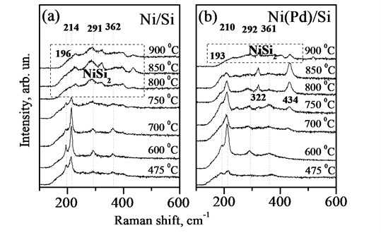
From Fig. 2(b) it is clear that the introduction of Pd in NiSi retards the formation of NiSi2 phase up to about °C, where the NiSi peaks at 193 and 210 cm-1 disappear, accompanying with the appearance of broad and diffuse peaks in the range of 200-450 cm-1, characteristic to NiSi2 structures [15, 16]. For comparison the full transformation to NiSi2 phase for NiSi sample already occurs at 800°C as the first-order Raman peak at 214 cm-1 disappears, while under critical transition condition of 750°C, we still have NiSi phase, although influenced by a certain amount of NiSi2 as peak broadening can be observed (Fig. 2(a)). Hence, the introduction of only 10 % of Pd to the initial nickel film can retard the formation of NiSi2 phase up to 900°С which is generally about 100-150°С more than that for pure NiSi film and in terms of thermal stability Ni(Pd)Si films are better suited for application in FBAR and MEMS that NiSi films in a wider range of thermal processing. A detailed additional study on temperature dependent Raman of NiSi and Ni(Pd)Si is reported in [17].
Both NiSi and Ni(Pd)Si films have proved to be polycrystalline in the result of experimental evaluation. As a matter of fact crystalline grains, oriented differently, influence the diffracted light and introduce the changes into Raman spectra [18]. By investigating Raman spectra and analysing the intensity ratio of the most intensive peaks (for Ni(Pd)Si and NiSi they are I210cm-1/I193cm-1 and I214cm-1/I196cm-1, respectively), one can qualitatively evaluate the degree of epitaxy of the film at microscopic level [18]. From Fig. 2 it is estimated that the intensity ratio changes from 1.62 to 4.25 for NiSi films, which reveals that there are grains of different orientations, and from 1.07 to 2.85 for Ni(Pd)Si films indicating a smaller dispersion of grain orientations for this film. Therefore, we can conclude that Ni(Pd)Si films are more homogeneous as the dispersion of the relative intensity values is smaller making this material better suited for the use as electrode material for FBARs and MEMS, and as silicide films are mainly polycrystalline it is crucial to have as smoother and aligned surface as possible.
Obtained micro-Raman measurements give the direct experimental evidence for the theoretical predictions in frames of nucleation theory which is used to explain the enhancement of nickel monosilicide stability by addition of various alloy elements [9, 11]. In general the transformation from nickel monosilicide to nickel disilicide is occurred via nucleation mechanism and Gibbs free energy for the reaction of:
can be written as:
In the presence of alloying metal М with the concentration of х the formation of NiSi2 should be altered by the following scheme [19]:
Therefore, Gibbs free energy of the reaction:
where determines mismatch entropy of the formation of solid state solution:
where – is a universal gas constant. As is negative, and the value of is positive, then is a more negative value than that of , resulting in a higher controlling force of the reaction (3), than that in reaction (5). Activation energy of the nucleation process at forming NiSi2 results from the equation:
where is the change of specific energy of surface tension and is the change of specific free Gibbs energy per unit volume. By absolute value , and therefore the activation energy is higher because of the presence of the solid state solution. Hence, the decrease in Gibbs free energy leads to the increase of nucleation energy, which explains the enhancement of thermal stability of the monosilicide phase in the system Ni1-xMxSi when annealing in comparison to pure NiSi.
Therefore in our case NiSi with the presence of Pd forms a solid state solution Ni1-xPdxSi. Since the decrease in Gibb’s free energy is smaller for Ni1-xPdxSi solid solution than that for pure NiSi, we expect a larger activation energy for NiSi2 nucleation. As a consequence, a higher formation temperature is needed to achieve NiSi2 phase in nickel alloy silicides.
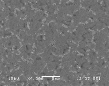
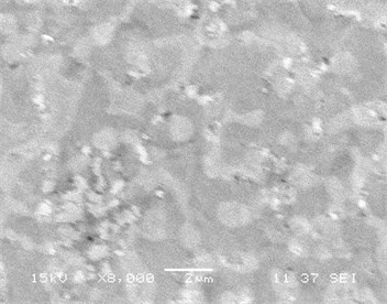
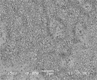
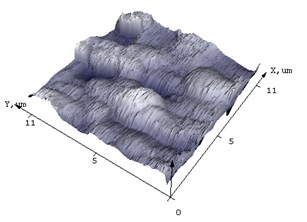
Fig. 3(a)-(d) displays a comparative study of surface morphology of nickel silicide and nickel palladium silicide film obtained by scanning electron microscopy measurements. In Fig. 3a-b SEM of both films are shown for low temperature annealing at 475°C, whereas Fig. 3c-d represent both films’ morphology at transition temperature of pure nickel silicides at 750°С.
It is clear that the surface of Ni(Pd)Si is relatively homogeneous and has a small-grain structure even at annealing temperature of 750 °С while the surface of NiSi film consists of inhomogeneously distributed huge grains that results in the process of phase transformation. Fig. 3 also indicates that Ni(Pd)Si film is polycrystalline with grains of a small size (about 100 nm and less). At lower annealing temperatures the surface of pure nickel silicide is more homogeneous than that of nickel palladium silicide that is explained by the going in process of palladium redistribution in the bulk of the sample.
Fig. 3SEM of films (а, c) NiSi and (b, d) Ni(Pd)Si on (111)Si at annealing temperatures T= 475 and 750 °С respectively
a)
b)
c)
d)
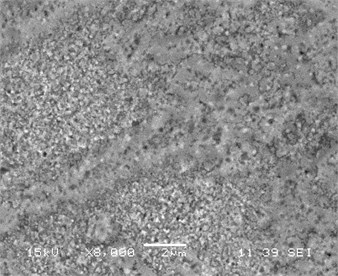
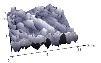
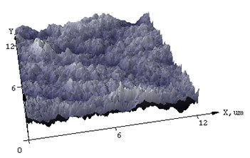
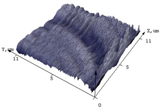
Fig. 4AFM of films (а, c) NiSi and (b, d) Ni(Pd)Si on (111) Si at annealing temperature T= 475 and 750°С respectively
a)
b)
c)
d)
Investigation of surface morphology together with phase analysis allows one to estimate the relative input of the resulting agglomeration of nickel silicide film or the transformation to nickel disilicide that influence the change of surface resistivity. As it is known the agglomeration of the silicide film can also impact the increase in surface resistivity, firstly due to the “holes” and silicon wafer exposure. In contrast to agglomeration process the increase in surface resistivity due to nickel disilicide formation occurs because of restructuring of the compound. In our case agglomeration represents the clustering of nickel particles in the film, when agglomerates of particles rigidly connected to each other appear that lead to the surface roughness, defects, islands growth and as a result the inhomogeneous resistivity of the film. Agglomeration occurs by means of linking the primary particles by Van-deer-Waals, Coulomb and other relatively weak interactions, primary particles keeping their form and size and stopping the formation of homogeneous film.
AFM was used to additionally characterize what changes the surface of the silicide film undergoes after annealing. In Fig. 4 the difference in morphology of NiSi and Ni(Pd)Si films is shown. The calculated from AFM results mean square roughness is at least 3 times less for alloyed films than that for pure NiSi and this tendency is unchanged even with the increase of annealing temperature. The structure of Ni(Pd)Si film surface is quite homogeneous, whereas for NiSi it is bumpy and represents a mountain chain like structure. Therefore we can conclude that the presence of Pd in nickel silicide substantially improves surface morphology of the film.
4. Conclusion
In this paper we have proved both experimentally and theoretically that the optimization of the most common used silicide in microelectronic technology by alloying with another metal will advance the creation of IC compatible film bulk acoustic resonators and microelectromechanical systems. We have investigated the main properties to be concerned: low resistivity of the film, thermal stability, high quality of the surface and low interface roughness. According to the experimental results, the resistivity of Ni(Pd)Si film is slightly higher than that of NiSi film, being low enough to be competitive with the latter. Moreover it is proved to be stable in a wider range of heat treatment temperatures which is crucial from technological point of view. Raman measurements allowed us to find out that phase transformation in Ni(Pd)Si is delayed up to 850-900°C in comparison with NiSi making it thermally more stable, which is theoretically explained in frames of change of Gibbs free energy. Besides the grains in the former film tend to be better aligned and less chaotically oriented, resulting in a smoother interface. AFM and SEM measurements have shown that surface of NiSi suffers severe agglomeration at high temperatures in comparison to Ni(Pd)Si films and has at least three times bigger mean square roughness, indicating that the alloying of nickel with Pd improves morphological stability of the silicide.
Thus, it seems that the best option for IC compatible film bulk acoustic resonators and microelectromechanical systems is Ni(Pd)Si film and not currently thought of NiSi film as the former has a smoother surface, is more thermally and morphologically stable with a constant surface resistivity in a wider temperature range of heat treatment.
References
-
Martin D. M., Enlund J., Yantchev V., Smith U., Olsson J., Katardjiev I. Thick silicides synthesised with smooth surface for integrated TFBAR applications. Proceedings of 22nd European Frequency and Time Forum, 2008, p. 6.
-
Cheung W. M., Cheng C. F., Poon M. C., Qin M., Yuen C. Y., Mansun C. New MEMS technology using multi-layer NILC poly-Si and NiSi films. Proceedings of Materials Research Society Symposium, Vol. 687, 2002, p. 1-6.
-
Nirschl M., Rantala A., Tukkiniemi K., Auer S., Hellgren A., Pitzer D., Schreiter M., Vikholm-Lundin I. CMOS-integrated film bulk acoustic resonators for label-free biosensing. Sensors, Vol. 10, 2010, p. 4180-4193.
-
Ramakoti Reddy P., Chandra Mohan B. Design and analysis of film bulk acoustic resonator (FBAR) filter for RF applications. International Journal of Engineering Business Management, Vol. 4, 2012, p. 1-4.
-
KunduA., DasS., Maity S., GuptaB., LahiriS., Saha H. A tunable band-stop filter using a metamaterial structure and MEMS bridges on a silicon substrate. Journal of Micromechanics and Microengineering, Vol. 22, 2012, p. 045004.
-
Qin M., Poon M. C., Yuen C. Y. A study of nickel silicide film as a mechanical material. Sensors and Actuators, Vol. 87, 2000, p. 90-95.
-
Lavoie C., D’Heurle F. M., Detavernier C., Cabral Jr. C. Towards implementation of a nickel silicide process for CMOS technologies. Microelectronic Engineering, Vol. 70, 2003, p. 144-157.
-
Zhang S.-L. Nickel-based contact metallization for SiGe MOSFETs: progress and challenges. Microelectronic Engineering, Vol. 70, 2003, p. 174-185.
-
Jin K. J., Pey K. L., Choi W. K., Antoniadis D. A., Fitzgerald E. A., Chi D. Z. Electrical characterization of platinum and palladium effects in nickel monosilicide/n-Si Schottky contacts. Thin Solid Films, Vol. 504, 2006, p. 149-151.
-
Kim D. S., Lee E. J., Kim J., Lee S. H. Low-cost contact formation of high-efficiency crystalline silicon solar cells by plating. Journal of the Korean Physical Society, Vol. 46, 2005, p. 1208-1212.
-
Huang W., Zhang L., Gao Y., Jin H. Effect of a thin W, Pt, Mo, and Zr interlayer on the thermal stability and electrical characteristics of NiSi. Microelectronic Engineering, Vol. 84, 2007, p. 678-683.
-
Hang Z., Yang B., Zhu Y., Gaudet S., Rossnagel S., Kellock A. J., Ozcan A., Murray C., Desjardins P., Zhang S.-L., Jordan-Sweet J., Lavoie C. Exploitation of a self-limiting process for reproducible formation of ultrathin Ni1−xPtx silicide films. Applied Physics Letters, Vol. 97, 2010, p. 252108.
-
Zhang Z., Zhang S.-L., Yang B., Zhu Y., Rossnagel S. M., Gaudet S., Kellock A. J., Jordan-Sweet J., Lavoie C. Morphological stability and specific resistivity of sub-10 nm silicide films of Ni1−xPtx on Si substrate. Applied Physics Letters, Vol. 96, 2010, p. 071915.
-
Donthu S. K., Tripathy S., Chi D. Z., Chua S. J. Raman scattering probe of anharmonic effects in NiSi. Journal of Raman Spectroscopy, Vol. 35, 2004, p. 536-540.
-
Zhao F. F., Chen S. Y., Shen Z. X., Gao X. S., Zheng J. Z., See A. K., Chan L. H. Applications of micro-Raman spectroscopy in salicide characterization for Si device fabrication. J. Vacuum Science and Technology B, Vol. 21, 2003, p. 862-867.
-
Li F., Lustig N., Klosowski P., Lannin J. S. Disorder-induced Raman scattering in NiSi2. Physics Review B, Vol. 41, 1990, p. 10210-10213.
-
Karabko A. O., Dostanko A. P., Kong J. F., Shen W. Z. Phase transition and phonon dynamics in NiPdSi: an annealing study by temperature-dependent Raman spectroscopy. Journal of Applied Physics, Vol. 105, 2009, p. 033518 (1-5).
-
Conti G., Lazik C., Uritsky Y. Micro-Raman сharacterization of phase formation and thermal stability of nickel silicide thin films. Microscopic Microanalysis, Vol. 11, 2005, p. 2094-2095.
-
Liu J. F., Chen H. B., Feng J. Y., Zhu J. Improvement of the thermal stability of NiSi films by using a thin Pt interlayer. Appl. Phys. Lett., Vol. 77, No. 14, 2000, p. 2177-2179.
About this article
A. Karabko would like to acknowledge the Belarusian Foundation for Fundamental Research, Grant T09M-041 and SPSR “Materials in Technology”, Grant 11-3049 for the support of this work.
