Abstract
Total ionizing dose (TID) irradiation impacts the device leakage currents or threshold voltage, which affects the single event transient (SET) vulnerability of electronics under radiation environment. SET response of SOI FinFET at 14 nm technology node after TID exposure is carried out at different dose level. Results show that the drain current peak presents a slight fluctuant with total dose, while the collected charge and the bipolar amplification coefficient first decrease with total dose and then increase. The potential reason is also discussed from competing mechanisms associated with decreasing threshold voltage from TID irradiation and increasing the drain diffuse current from the potential of the channel.
1. Introduction
When an energetic ion hits the sensitive area of semiconductor device, single event transient (SET) may occur. With device feature size scaled down, SET plays an important role on the analysis of the reliability for integrated circuits under radiation environment [1-3]. As device feature size goes down into sub-micro or nanometer regime, short channel effects (SCEs), like drain induced barrier lowering (DIBL), degradation of off current, have become a serious concern for the device performances [4-6]. Fin-type field-effect-transistor (FinFET) is one of the emerging non-planar and multi-gate devices. Because of its higher speed, higher density, higher scalability and lower power, FinFET has been paid much attention for one of the most promising candidates to replace current CMOS technologies [7]. The sensitive of FinFETs to total ionizing dose (TID) effect can be reduced by thin silicon fins [7-9]. Although silicon-on-insulator (SOI) technology is helpful for improving the tolerance of devices to SET, the sensitivity of SOI device to TID is also serious due to the existence of oxide insulator [7-9]. Therefore, electronics devices for space environments experience TID and SET simultaneously [10-13]. Some simulation and experimental results have indicated that the SET pulse width and the sensitive area decrease due to heavy-ion induced dose for the IBM 180nm process [10]. However, for a 130 nm SRAM and the SEU- and SET-induced soft errors in 40-nm bulk circuits, the experimental results have shown increases in the neutron SEU cross section caused by TID irradiation [10].
In this work, the effect of TID on the response of SET for SOI FinFET at 14 nm technology node is explored. The paper is organized as follows: Section 2 presents the simulation model of SOI FinFET at 14 nm technology node. The impact of TID on SET is simulated and analyzed in Section 3. Section 4 concludes the paper.
2. Device model for FinFET
Based on TCAD, a 3D model of SOI FinFET at 14 nm technology node is simulated, shown in Fig. 1. The simulation parameters of the device are from ITRS 2013, shown in Table 1. Somephysical models are included. For simulating the presence of interface traps at the silicon/oxide interface, the direct recombination model is used. Compared with the density gradient model, the Bohm quantum potential (BQP) model converges and calibrates to the Schrodinger-Poisson model well. Therefore, BQP is used to model the effect of quantum mechanical confinement [14]. For obtaining the velocity saturation effect, the high-field saturation mobility model is also recommended. Because of the thermal generation, the devices always have the leakage currents, which is simulated by the Shockley-Read-Hall (SRH) recombination model. Along with the remote Coulomb scattering mobility model, the remote phonon scattering mobility model is included to describe the mobility reduction observed in high k gate dielectric FET devices [14]. For MOSFET, the degradation of the electron or hole mobility occurs inside inversion layers. To capture the correct performances of MOSFET, an inversion layer model from Lombardi is used.
When the SOI device behaves like a bipolar transistor, the band gap narrowing model is recommended to accurately simulate the bipolar current gain. To accurately simulate the impact ionization effect, we use a non-Maxwellian based model from Concannon. The Fermi-Dirac statistics are also selected to obtain the certain properties of very highly-doped devices.
The model of single event transient simulation due to an energetic particle strike is used [14]. The supply voltage is set to 0.8 V. The simulation result is good agreement with the experimental data of n-type SOI FinFET [15], as shown in Fig. 2.
Table 1Parameters of 14nm SOI FinFET
Parameter | Value | Parameter | Value |
Length of gate | 14 nm | Length of source/drain region | 35nm |
Fin height | 18 nm | Length of extent source/drain region | 33nm |
Fin width | 10 nm | Gate dielectric material | SiO2 |
Eox | 2 nm | Contact material | Si3N4 |
Channel doping concentration | 5×1015 cm-3 | Extent source/drain doping concentration | 8×1019 cm-3 |
Source/drain doping concentration | 1×1021 cm-3 | Substrate doping concentration | 1×1015 cm-3 |
Fig. 1Structure of 14 nm FinFET device
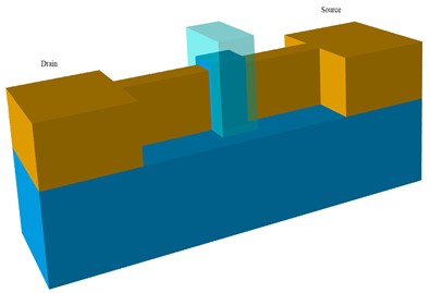
Fig. 2I-V electrical character curve for model and experiment results [15]
![I-V electrical character curve for model and experiment results [15]](https://static-01.extrica.com/articles/23602/23602-img2.jpg)
3. SET response of FinFET after TID
The effect of TID on SET sensitivity of 14nm SOI FinFET is studied. The device is at “off” state for 10 keV X-ray irradiation. The results of pre- and after irradiation are shown in Fig. 3.
It is clear that as the captured positive oxide trap charges in the SiO2 increase, the threshold voltage decreases [16]. After irradiation, the supply voltage of the device being 0.8 V, the drain currents for different linear energy transfer (LET) are shown in Fig. 4.
Fig. 3IDS-VGS curves for pre-irradiation, 50 krad (SiO2), 100 krad (SiO2), 500 krad (SiO2) and 1Mrad (SiO2) irradiation
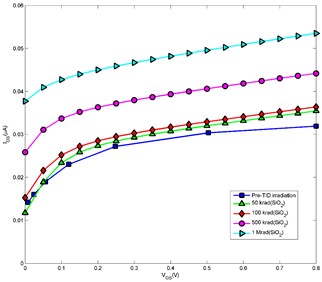
Fig. 4Drain current for different LET of after irradiation device
a) 50 krad (SiO2)
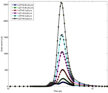
b) 1 Mrad (SiO2)
For quantifying the influence of TID irradiation on the SET response of FinFET, the collected charger and the bipolar amplification coefficient are defined as below [17]:
where, is the collected charge, is the simulated drain current of the device, is the bipolar amplification coefficient, is the deposited charge that can be obtained considering the Gaussian distribution of the ion track and the 3D geometry of the silicon body [18], and is the simulation time.
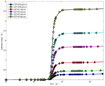
The collected charge is shown in Fig. 5. The comparison results of SET responses for different LET of FinFET after 50 krad (SiO2) and 1 Mrad (SiO2) irradiation are shown in Fig. 6, respectively.
It can be concluded that as total dose level is increased, the drain current peaks of FinFETs under the same LET conditions are slight fluctuant [19]. Their current peaks nearly increase with increasing LET linearly. However, with total dose level increasing from 50 krad (SiO2) to 1 Mrad (SiO2), the devices get a trend of first decrease then increase in the drain collected charge [10]. The reason may be that due to TID irradiation, the threshold voltage of the device reduces, which leads to the driven current of the device increase. A larger driven current gets a good immunity to SET [16, 20], resulting in the collected charge decrease. Simultaneously, after TID irradiation, large numbers of the positive hole trap charges are captured by the gate oxide [16]. Therefore, the potential of the channel is increased, resulting in that the drain diffuse current is enhanced. This fact leads to the collected charge increase. Based on the above analysis, due to competing mechanisms associated with decreasing threshold voltage and increasing the drain diffuse current, the collected charge first decreases with total dose and then increases. When LET is less than 10 pC/μm, due to TID irradiation, the device gets a significant increase in the bipolar amplification effect. The bipolar amplification coefficient can be obtained by the ratio between the collected charge and the deposited charge [17]. As LET increases, the bipolar amplification coefficient decreases and in the trend of a slight impact by the irradiation.
Fig. 5Collected charge for different LET of after irradiation device
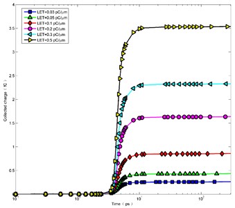
a) 50 krad (SiO2)
b) 1 Mrad (SiO2)
Fig. 6SET response of device after irradiation
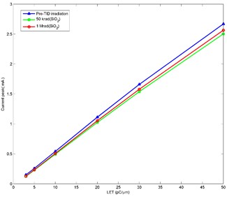
a) Current peak
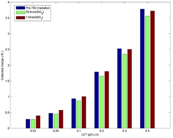
b) Collected charge
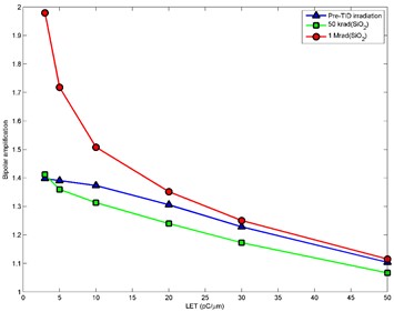
c) Bipolar amplification coefficient
4. Conclusions
TID irradiation may change the transistor leakage currents or threshold voltage and then impacts SET sensitivity of the devices. The effect of TID on SET response of SOI FinFET at 14 nm technology node is investigated with irradiations at different dose levels. The results show that as total dose increases, the drain current peak under the same conditions present a slight fluctuant, while the collected charge and the bipolar amplification coefficient first decrease and then increase. The potential mechanism is also discussed.
References
-
L. Artola, M. Gaillardin, G. Hubert, M. Raine, and P. Paillet, “Modeling single event transients in advanced devices and ICs,” IEEE Transactions on Nuclear Science, Vol. 62, No. 4, pp. 1528–1539, Aug. 2015, https://doi.org/10.1109/tns.2015.2432271
-
M. Saremi, A. Privat, H. J. Barnaby, and L. T. Clark, “Physically based predictive model for single event transients in CMOS gates,” IEEE Transactions on Electron Devices, Vol. 63, No. 6, pp. 2248–2254, Jun. 2016, https://doi.org/10.1109/ted.2016.2547423
-
P. Caron et al., “Physical mechanisms inducing electron single-event upset,” IEEE Transactions on Nuclear Science, Vol. 65, No. 8, pp. 1759–1767, Aug. 2018, https://doi.org/10.1109/tns.2018.2819421
-
M. Saremi, A. Afzali-Kusha, and S. Mohammadi, “Ground plane fin-shaped field effect transistor (GP-FinFET): A FinFET for low leakage power circuits,” Microelectronic Engineering, Vol. 95, No. 2, pp. 74–82, Jul. 2012, https://doi.org/10.1016/j.mee.2012.01.009
-
R. Saha, B. Bhowmick, and S. Baishya, “Si and Ge step-FinFETs: work function variability, optimization and electrical parameters,” Superlattices and Microstructures, Vol. 107, pp. 5–16, Jul. 2017, https://doi.org/10.1016/j.spmi.2017.04.001
-
“International Technology Roadmap for Semiconductors (ITRS).” Semiconductor Industry Association, http://www.itrs.net/links/2013itrs/home2013.htm
-
W. Wu et al., “Line-edge roughness induced single event transient variation in SOI FinFETs,” Journal of Semiconductors, Vol. 36, No. 11, p. 11400, 2015.
-
P. Roche et al., “Technology downscaling worsening radiation effects in bulk: SOI to the rescue,” in 2013 IEEE International Electron Device Meeting, pp. 766–769, 2013.
-
M. Gaillardin, P. Paillet, V. Ferlet-Cavrois, S. Cristoloveanu, O. Faynot, and C. Jahan, “High tolerance to total ionizing dose of Ω-shaped gate field-effect transistors,” Applied Physics Letters, Vol. 88, No. 22, p. 22351, May 2006, https://doi.org/10.1063/1.2206097
-
H. Zhang et al., “Effects of total-ionizing-dose irradiation on single-event response for flip-flop designs at a 14-/16-nm bulk FinFET technology node,” IEEE Transactions on Nuclear Science, Vol. 65, No. 8, pp. 1928–1934, Aug. 2018, https://doi.org/10.1109/tns.2017.2781622
-
A. S. Cardoso et al., “Single-Event Transient and Total Dose Response of Precision Voltage Reference Circuits Designed in a 90-nm SiGe BiCMOS Technology,” IEEE Transactions on Nuclear Science, Vol. 61, No. 6, pp. 3210–3217, Dec. 2014, https://doi.org/10.1109/tns.2014.2358078
-
J.-X. Zhang et al., “Synergistic effect of total ionizing dose on single event effect induced by pulsed laser microbeam on SiGe heterojunction bipolar transistor,” Chinese Physics B, Vol. 27, No. 10, p. 108501, Oct. 2018, https://doi.org/10.1088/1674-1056/27/10/108501
-
Y.-N. Yin et al., “Influences of total ionizing dose on single event effect sensitivity in floating gate cells,” Chinese Physics B, Vol. 27, No. 8, p. 086103, Aug. 2018, https://doi.org/10.1088/1674-1056/27/8/086103
-
ATLAS User’s Manual. SILVACO International Inc, 2012.
-
C.-H. Lin et al., “High performance 14nm SOI FinFET CMOS technology with 0.0174 μm2 embedded DRAM and 15 levels of Cu metallization,” in 2014 IEEE International Electron Devices Meeting (IEDM), Dec. 2014, https://doi.org/10.1109/iedm.2014.7046977
-
Zhuo Qing-Qing, Liu Hong-Xia, and Wang Zhi, “Single event effect of 3D H-gate SOI NMOS devices in total dose ionizing,” (in Chinese), Acta Physica Sinica, Vol. 62, No. 17, p. 176106, 2013, https://doi.org/10.7498/aps.62.176106
-
B. Liu, C. Li, C. Li, and S. Zhang, “Effect of temperature and single event transient on crosstalk in coupled single‐walled carbon nanotube (SWCNT) bundle interconnects,” International Journal of Circuit Theory and Applications, Vol. 49, No. 10, pp. 3408–3420, Oct. 2021, https://doi.org/10.1002/cta.3089
-
D. Munteanu and J. L. Autran, “3D simulation of single-event-transient effects in symmetrical dual-material double-gate MOSFETs,” Microelectronics Reliability, Vol. 55, No. 9-10, pp. 1522–1526, Aug. 2015, https://doi.org/10.1016/j.microrel.2015.07.022
-
B. Liu, C. Li, P. Zhou, and J. Zhu, “Analysis of location and LET dependence of single event transient in 14 nm SOI FinFET,” Nuclear Instruments and Methods in Physics Research Section B: Beam Interactions with Materials and Atoms, Vol. 530, No. 8, pp. 13–17, Nov. 2022, https://doi.org/10.1016/j.nimb.2022.09.008
-
R. C. Harrington et al., “Effect of transistor variants on single-event transients at the 14-/16-nm bulk FinFET technology generation,” IEEE Transactions on Nuclear Science, Vol. 65, No. 8, pp. 1807–1813, Aug. 2018, https://doi.org/10.1109/tns.2018.2843260
About this article

This work was supported by the National Natural Science Foundation of China under Grant No. 11975311, 11405270 and Foundation of Independent Scientific Research of Air Force Engineering University under Grant No. YNJC19070504.
The datasets generated during and/or analyzed during the current study are available from the corresponding author on reasonable request.
The authors declare that they have no conflict of interest.
