Abstract
Thermal relaxation differential spectrometry (TRDS) was used to study the thermal parameters of samples with various design features for heat removal - a powerful LED lamp (150 W) used in industrial and street lighting, low power LED lamps (4 W) with filament emitters, as well as SMD emitter. It is shown that the method of thermal relaxation differential spectrometry is effectively applicable to the study of the structure of thermal parameters of both high-power and low-power LED devices. The method is informative and allows to study in the distribution of thermal resistance and heat flux over the volume and layers of the LED device detail. The use of the TRDS method allows the optimization of the thermal design of LED devices to reduce the overheating temperature of their active regions, and, therefore, to reduce the degradation of LED devices.
1. Introduction
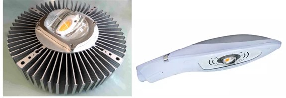
Thermal parameters were studied for a sample of a CD-RL850-150 high-power LED lamp, manufactured by Cedar Electronics, used in industrial and street lighting. The active element of the lamp is an integrated matrix of the CXM22 type of chip on board (COB) technology with a color temperature of 2200K. For comparison, similar studies were performed low power lamps. The analysis of the thermal parameters of the measured sample was carried out by the method of thermal relaxation differential spectrometry (TRDS) using a relaxation impedance spectrometer developed at the Belarusian National Technical University (BNTU) [1, 2]. In the TRDS method, as opposed to the known methods that use the structure-function and the differential structure function [2-17], as well as those included in the standard [18], the output of measurement results of the thermal parameters of the measured samples is carried out in the form of a spectrum of thermal parameters, similar to conventional types of spectrum, for example, optical. This type of data presentation is quite informative and convenient for analyzing measurement results. Besides, the TRDS method allows one to obtain a profile of the distribution of the effective cross-section of the heat flux along with the propagation of heat in the sample. The TRDS method uses an original algorithm for direct differential transformation of the transient equations of dynamic thermal impedance into electrothermal models in the time domain, bypassing frequency transformations (frequency deconvolution) powerful LED lamps with filament emitters, as well as with SMD emitters.
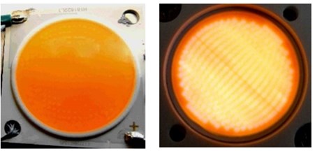
Fig. 1External view of the a) CD-RL850-150 lamp and b) the COB matrix
a)
b)
2. Experimental technique
The measurements were carried out in the operating mode of power supply for this type of lamp 2.4 A, 55 V, 20 °C, in various modes: in the LED position with the emitter up and down; with different degrees of clamping of the COB matrix; with active ventilation of the radiator and without ventilation. When calculating the thermal resistance of the lamp, the power efficiency was taken to be 0.5.
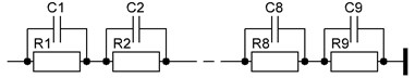
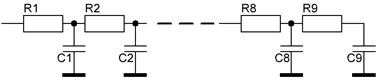
In the sample under study, the profile of the distribution of the heat flux from the active layer to the external environment, the thermal time constants of the elements of the device cases, and the structure of thermal resistance in the form of a discrete and continuous spectrum are determined. The continuous spectrum is calculated on the basis of the higher-order derivatives of the dynamic thermal impedance and corresponds to the Foster model (Fig. 2(a)), and the discrete spectrum is calculated on the Cayer model (Fig. 2(b)) according to the principle of electrothermal analogy.
Fig. 2a) Thermal RC model of Foster and b) of Cayer in accordance with the concept of the electro-thermal analogy
a)
b)
Analysis of the measurement results of the overheating temperature during self-heating and cooling of the sample based on the representation of its structure as an equivalent thermal RC circuit for multilayer systems allows one to determine the value and structure of the thermal resistance of a semiconductor device. For analysis within the framework of the Foster model, the logarithmic time derivatives of the dynamic thermal resistance are determined, defined as . Higher-order derivatives ( 1) are used to increase the temporal resolution of the structural components with close :
This approach allows us to increase the number of devices resolved within the framework of the method of thermal structural elements to 10-12 (sources mention 3-5). Further, this differential spectrum obtained within the framework of the Foster model is recalculated into a discrete spectrum within the framework of the Cayer model, which corresponds to the real processes of heat propagation in the device to a greater extent.
Additionally, the analysis of the spreading of the heat flux in the structures under study was carried out based on the concept of thermal diffusivity (thermal effusion). To determine the spreading area of the heat flux along with the structure of the semiconductor device, the ratio between the thermal resistance and the heat capacity of the layers of the components of the device structure is used:
Thus, knowing the , , parameters of the structure layers, the thermal resistance and the heat capacity of the layers , obtained from the discrete thermal spectrum, it is possible to determine the distribution of the cross-sectional area of the heat flux from the crystal surface to the external environment.
From the layer-by-layer values of the components of thermal resistance and heat capacity, the effective cross-sectional area of the heat flux (Sе) in the structure under study, and the profile of its distribution from the active layer to the outer boundary of the sample under study were determined [1].
The time sweep of the TRDS spectra was 10 orders of magnitude from the initial point and was performed in the interval (heating/cooling) ≤ 104с and a resolution of 2·10-6с, which corresponds to the relaxation times of heat on the internal thermal resistance of the sample under study.
3. Experiments, analysis, and discussion of measurement results
As a first approximation, when studying layer-by-layer heat spreading, the layer structure of a CD-RL850-150 lamp can be represented (Fig. 3) as a sequential model with six functional elements:
1. Multiple LED crystal (n-LED chip).
2. Attachment zone (usually by soldering) of the crystal (Die Attach) on the substrate.
3. PCB printed circuit board (printed circuit board).
4. DBC sintered substrate (Direct Bond Copper).
5. TIM paste – thermal interface material.
6. Heat radiator.
An estimate shows that thermal scattering through the phosphor and the lens is insignificant in relation to scattering in other parts of the lamp and was not taken into account in the analysis.
From the analysis of the time dependence of the temperature of the active region of the COB matrix by the TRDS method, the thermal parameters of the measured sample and its structure in the form of discrete and continuous spectra (depending on the thermal relaxation time constant) and the distribution profile of the effective cross-section of the heat flux from the active region of the lamp to the environment are found (Fig. 4).
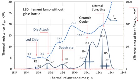
Fig. 4 shows the spectra of thermal parameters of the CD-RL850-150 lamp obtained from measurements in the upward emitter position and in additional modes with the forced blowing of the radiator (air blow) and with a weakened clamping of the COB matrix to the radiator (poor contact). Discrete spectra, in the form of vertical dashes, correspond to the Cayer model, and the continuous ones correspond to the Foster model. For the investigated lamp, the spectral resolution was set, sufficient for constructing 9-link (9th order) electrothermal RC-models. Such discretization of the spectra is quite informative for a given type of sample and it is relatively easy to interpret the structure of a given sample. Figure 4 also shows the distribution of the effective cross-section of the heat flux for the convenience of interpretation and identification and analysis of zones of inhomogeneous heat relaxation Se(τ). Following the specified resolution of the model, 9 layer components, inhomogeneous in thermal parameters, for the internal thermal resistance of the lamp, designated as R1-R9, were identified on the spectra. From the analysis of the TRDS spectra, the components of the layered structure of the lamp are identified as follows: R1 and R2 are the thermal resistances of the surface and volume of the crystal, respectively; R3 – crystal and PCB layer landing zones; R4 - TIM layer; R5, R6, R7, - internal resistance of the radiator heatsink; R8 and R9 are the resistances of the radiator – external medium transition region. Components R1-R3, located in the initial spectral region in the 0.01-2 ms time range, corresponding to the COB matrix.
Fig. 3Schematic structure of the CD-RL850-150 lamp
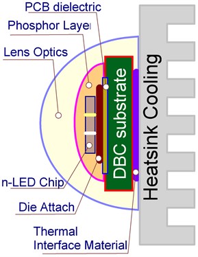
Fig. 4 shows that the most significant contribution to the total thermal resistance is made by the resistance of the radiator, which is associated with the design features of this radiator in its inner part near the border with the COB matrix. It is also seen that the effective area and its distribution , for the heat flux, are significantly lower than the theoretically possible one, determined by the geometric dimensions of this area. For example, it follows from measurements, that in the middle area of the LED chip = 125 mm2, which is about 30 % of the geometric area of this area. This can be attributed to the discreteness of the LED crystal itself and the inhomogeneous distribution of the current density in the cross-section of the crystal. Further, as can be seen in Fig. 4, in the time interval of 1-10 ms (in the zone of the crystal landing), a narrowing of the heat flux occurs, which is called a thermal bottleneck. This effect is caused, as a rule, by the poor quality of the crystal fit due to defects in the soldering zone. A significant increase in the thermal inhomogeneity of this layer can lead to the appearance of regions of local overheating, i.e. hot spots, at the crystal-solder interface. Then, in time ( 10-100 ms), a relatively monotonic increase in the spreading of the heat flux to the next thermal barrier, the TIM layer, is observed in the DBC metal-ceramic substrate. In this region, the cross-sectional area of the heat flux is approximately equal to the geometric area of the crystal – 300 mm2. In a similar way, the spreading of the heat flux occurs in zones with increased thermal inhomogeneity in the inner region of the radiator ( 1-20 s) and at its border with the environment ( 200-1000 s). In the final region of heat spreading into the environment, the effective cross-sectional area of the heat flux is significantly lower than the area of the radiator fins, which indicates its low thermal efficiency. For unambiguous identification in the TRDS spectra of the layer structure, additional measurements were carried out in the mode with the forced blowing of the radiator and in the mode with a weakened pressing of the COB matrix to the radiator (red dotted lines in Fig. 4). As can be seen from the figure, this made it possible to accurately identify the position of the TIM layer (R4) and the heatsink – external environment (R8, R9) boundaries in the obtained spectra. It is also obvious that the use of active cooling (blowing of the heatsink fins) significantly lowers the thermal barrier in the transition layer at the heatsink – external environment (R8) interface, and weak pressing of the COB matrix to the substrate leads to an increase in the transition thermal resistance R4 of the TIM layer.
Fig. 4Discrete (vertical lines) and differential (continuous monotone line) thermal resistance spectra Rthτ of CD-RL850-150 lamp. Distribution of thermal flow cross-section Seτ over thermal relaxation times (secondary scale)
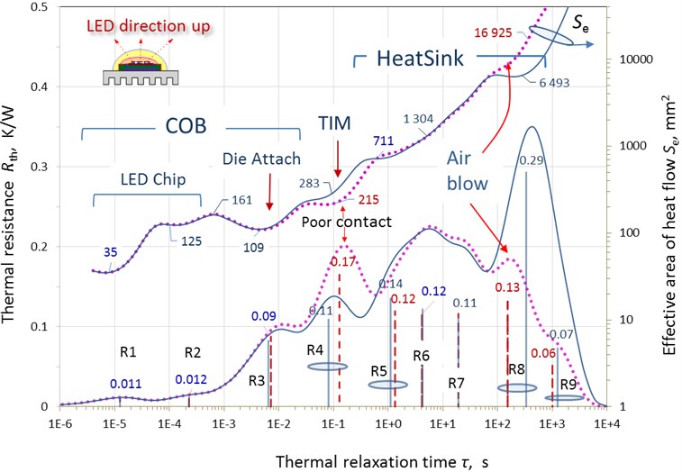
Fig. 5 shows comparative spectra of thermal parameters obtained at 2 lamp positions – emitter up and down.
It can be seen from the figure that when the lamp is directed downward, the internal resistance of the radiator decreases mainly due to the components R6 and R7, and the lateral spreading of heat in this region of the radiator increases.
Table 1Experimental thermal characteristics of CD-RL850-150 lamp structure components
Layer components | Thermal resistance , K/W | Thermal relaxation time |
LED die | 0.023 | 0.21 ms |
Die attach | 0.09 | 6.5 ms |
COB | 0.12 | 6.8 ms |
TIM | 0.11 | 0.082 s |
Heatsink* | 0.63 / 0.74 / 0.54 | 1700 s |
of lamp* | 0.85 / 0.95/ 0.75 | |
*LED down/ LED up/ LED up +active cooling | ||
The numerical values of the thermal parameters for individual layers of the lamp at different positions and modes of lamp cooling are summarized in Table 1.
Fig. 5Thermal resistance spectra Rthτ and the distribution of thermal flow cross-section Seτ (secondary scale) over thermal relaxation times. Red lines – LED light direction down, blue lines – LED up
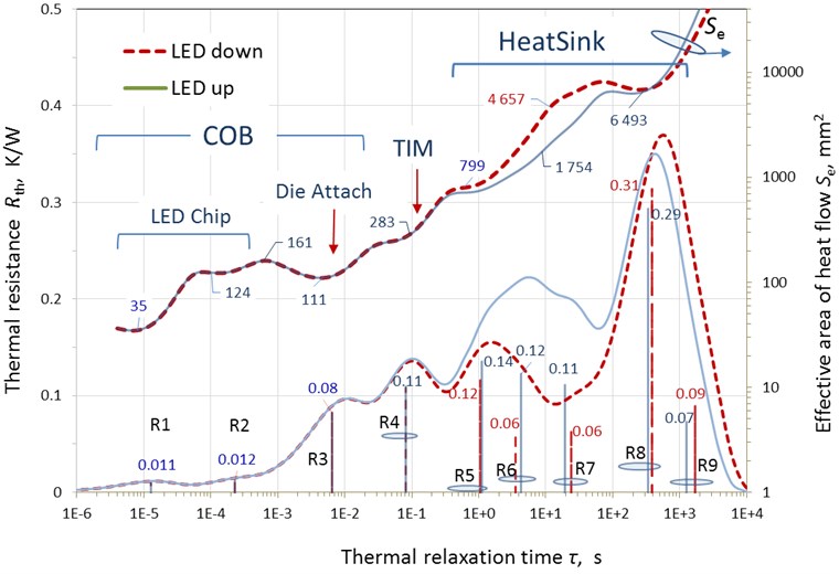
Fig. 6Overheating temperature of LED dies (continuous monotone line) and discrete spectra of the overheating temperature (vertical lines)
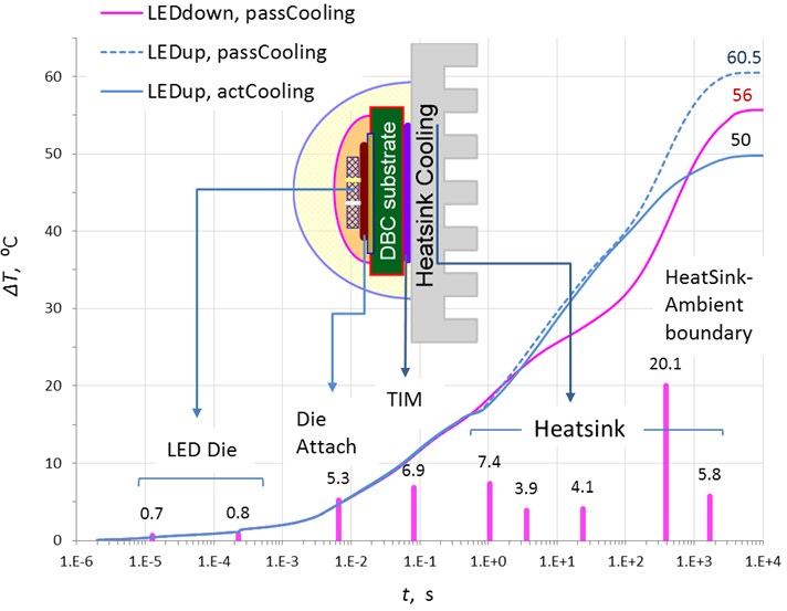
Fig. 6 shows the measured time dependence of the overheating temperature of the active region of the lamp (continuous line in the graph) and the discrete-time spectrum of the overheating temperature (vertical lines) for the cases of cooling the radiator by natural convection of air, passive cooling (dash line) and forced blowing active cooling (blue), as well as in the upward emitter position with passive cooling (red).
It can be seen from the figure that monotonically increases during the first 2 hours after switching on under load and reaches a level of 61°C with passive cooling and 50 °C with active cooling. In the position of the lamp with the emitter downward, the overheating temperature is 55-56 °С without forced cooling. The thermal (Joule) power dissipated by the lamp was 65 W. From the figure, it is also possible to estimate the discrete distribution of the overheating temperature change on various elements of the lamp.
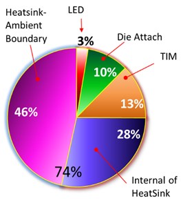
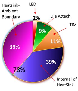
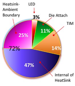
The structure of the relative distribution of the thermal resistance of various lamp elements is shown in Fig. 7 in the form of a circular diagram.
Fig. 7Diagrams of the contribution of the thermal resistances of various layers in the structures of CD-RL850-150 lamp: a) LED light direction up; b) LED down; (a) LED up +active cooler
a)
b)
c)
It can be seen from the diagram that the greatest contribution to the total thermal resistance of the lamp is made by the resistance of the radiator, which in different measurement modes is from 72 to 78 % .
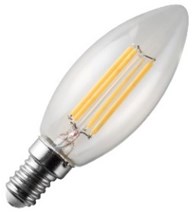
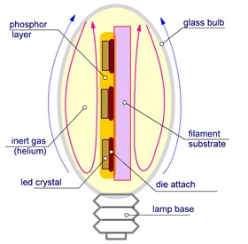
A change in the structure of the thermal resistance of a LED lamp (~4 W) with filament emitters (Fig. 8), associated with the degradation or depressurization of its bulb, was studied. The bulb of a filament lamp is filled with an inert gas (helium) with high thermal conductivity. The appearance and schematic structure of the lamp is shown in Fig. 8.
Fig. 8Appearance of the studied lamp with filament emitters and its schematic structure
a)
b)
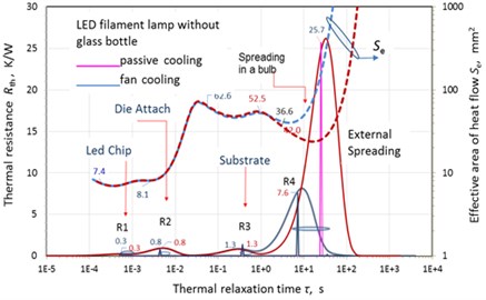
Fig. 8 shows 5 main components of the structure of a filamentous LED lamp, which determine the total thermal resistance of the sample under study – LED crystal, crystal fit, filamentous substrate, thermal resistances of spreading in a gaseous medium in the lamp bulb and into the external environment. The spread of heat in the lamp through the phosphor, as a rule, is not significant and was not taken into account in the analysis.
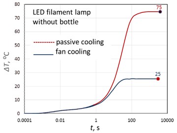
Fig. 9 shows the time dependences of the overheating temperatures, as well as the TRDS spectra of the lamp with and without a bulb and the result of their discretization within the Cayer model. It can be seen that after 1 s after switching on, significant heating of the lamps begins, and after 100 s, the lamps go to a stationary mode. The overheating temperature of the original lamp reaches 58 °C, the same lamp without the bulb is 75 °C.
Discretization of the spectra (Fig. 9) was carried out within the framework of the model corresponding to the schematic structure in Fig. 8. Accordingly, on the discrete TRDS spectra, R1 is identified as the thermal resistance of light-emitting diode (LED) crystals, R2 belongs to the crystal landing layer, R3 is the thermal resistance of sapphire whiskers. Thermal resistance R4 is associated with the spreading of heat in the glass bulb of the lamp over helium. Thermal resistance R5 is associated with the spreading of heat into the environment. The effective area of the heat flux is narrowed as heat spreads inside the bulb. This is probably due to the presence of hotter regions on the opposite side of the sapphire substrates opposite to the LEDs.
Fig. 9Dependence of the overheating temperature of the original lamp and the lamp without a bulb on time and the corresponding spectra of thermal resistances
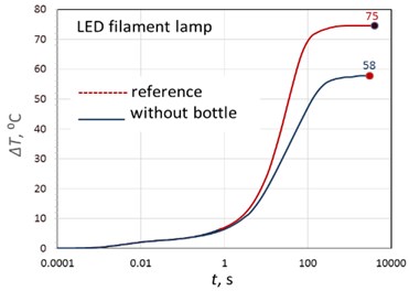
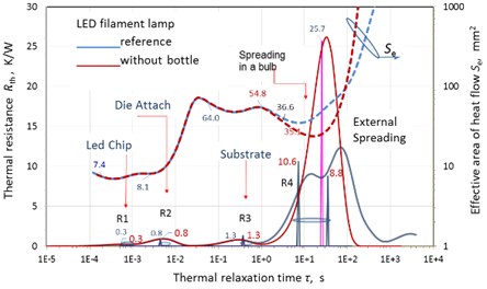
Fig. 9 shows that when the glass bulb is removed (or in the case of its degradation, leading to the replacement of helium with air), the thermal resistance R4 to the external environment sharply increases and the heat flux area in the R4 region decreases even more due to the much lower thermal conductivity of air.
Fig. 10Dependence of the overheating temperature of the original lamp on time with passive and active cooling
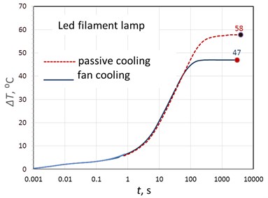
To check the efficiency of heat removal in the lamp, a forced airflow was carried out both for the original lamp and for the lamp without a bulb. It should be noted that the temperature of overheating of the active area of the LED of the original lamp, as a result of blowing decreased slightly (from 58 °С to 47 °С) (Fig. 10).
At the same time, the overheating temperature of the lamp without the bulb dropped significantly (Fig. 11).
Fig. 11Dependence of the overheating temperature of the lamp without the bulb on time and the corresponding spectra of thermal resistances with passive and active cooling
These facts indicate a good thermal design of the lamp, i.e. the presence of helium inside of the flask gives an effect comparable to forced cooling. In the TRDS spectra in Fig. 11, one can see the corresponding changes in the thermal resistances R4, R5. Depressurization of the bulb (i.e. replacing helium with air) significantly increases the temperature of the active region of the lamp, thus increasing the likelihood of its degradation.
For comparison, the thermal design of a standard SMD (surface-mount device) lamp (~4 W) with surface-mount LEDs was also investigated. Thermal measurements of an SMD lamp were made without a light diffuser.
Fig. 12 shows the appearance of an SMD lamp without a light diffuser and a schematic structure of this type of lamp.
Fig. 12External view of a LED lamp with an SMD emitter and its schematic structure
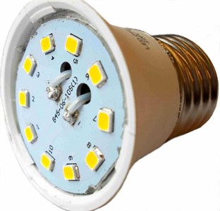
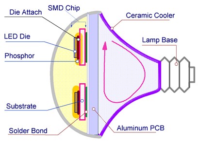
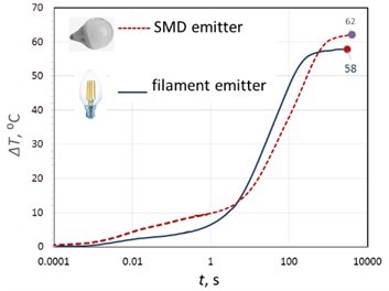
Fig. 13 shows the time dependences of the overheating temperatures of the SMD emitter and the filament lamp, as well as the TRDS spectra of the SMD lamp and the result of their discretization within the Cayer model. It can be seen that 5 s after switching on, significant heating of the emitter of the SMD lamp begins, and it takes more than an hour to reach the stationary mode. For an SMD lamp, these times are significantly longer than for a filament lamp, which is explained by the presence of a ceramic radiator, which significantly increases the thermal inertia of the entire lamp. The overheating temperature of an SMD lamp reaches 61 °C, which is comparable to the temperature of a lamp with a filamentous emitter of 58 °C. With a short-term switch-on, in the interval of 5-500 s, the overheating of the filament emitter is greater than that of the SMD lamp, and with a longer switch-on of the SMD lamp, the lamp heats up more (Fig. 13(a)).
Fig. 13Dependences of the overheating temperature of an SMD lamp and a lamp with a filamentous emitter on time and the spectra of thermal resistances of an SMD lamp
а)
b)
The discretization of the TRDS spectra of an SMD lamp was carried with its structure taken into account (Fig. 12) in the same way as for a filament lamp. Analysis of the spectra of this lamp shows a significant contribution of the radiator (R4, R5) to the thermal resistance of the lamp. Fig. 13(b) shows that in the range of the radiator spectrum there is a narrowing of the heat flux in the form of a characteristic “bottleneck”, which indicates the presence of zones of uneven heating and, as a consequence, low thermal efficiency of this radiator.
4. Conclusions
Based on the results of the study of the thermal interface of the CD-RL850-150 lamp with filament emitters and SMD emitters, the original method (TRDS), developed at the Belarusian National Technical University, the following was established:
1) The method of thermal relaxation differential spectrometry is effectively applicable to the study of the structure of thermal parameters of powerful large-sized LED devices.
2) The method allows you to study the distribution of thermal resistance and heat flux over the volume and layers of the LED device in detail.
This method of studying the detailed structure of the thermal resistance of super-power LED devices is highly informative.
The use of the TRDS method will optimize the thermal design of ultra-high-power LED devices to reduce the overheating temperature of their active regions, and, therefore, reduce the degradation of LED devices.
References
-
A. L. Zakgeim, A. E. Chernyakov, A. S. Vaskou, V. K. Kononenko, and V. S. Niss, “Comparative analysis of the thermal resistance profiles of power light-emitting diodes cree and rebel types,” in 2013 14th International Conference on Thermal, Mechanical and Multi-Physics Simulation and Experiments in Microelectronics and Microsystems (EuroSimE), Apr. 2013, https://doi.org/10.1109/eurosime.2013.6529922
-
Yu. A. Bumai, A. S. Vaskou, V. K. Kononenko and V. M. Lomako, “Relaxation impedance spectrometer of thermal processes,” Electron. info, Vol. 3, pp. 58–59, 2010.
-
G. Farkas et al., “Electric and thermal transient effects in high power optical devices,” in Twentieth Annual IEEE Semiconductor Thermal Measurement and Management Symposium, 2004, https://doi.org/10.1109/stherm.2004.1291320
-
Shang-Ping Ying and Wei-Bo Shen, “Thermal analysis of high-power multichip COB light-emitting diodes with different chip sizes,” IEEE Transactions on Electron Devices, Vol. 62, No. 3, pp. 896–901, Mar. 2015, https://doi.org/10.1109/ted.2015.2390255
-
P. Anithambigai, D. Mutharasu, T. Zahner, L. H. Huong, and D. Lacey, “A comparison study on thermal characterization of high power leds with different ceramic attach adhesives for automotive lighting applications,” in 2014 20th International Workshop on Thermal Investigations of ICs and Systems (THERMINIC), Sep. 2014, https://doi.org/10.1109/therminic.2014.6972521
-
P. Zhang, J. Zeng, X. Chen, M. Cai, J. Xiao, and D. Yang, “An experimental investigation of a 100-W high-power light-emitting diode array using vapor chamber–based plate,” Advances in Mechanical Engineering, Vol. 7, No. 11, Nov. 2015, https://doi.org/10.1177/1687814015620074
-
A. Poppe, E. Kolla, Z. Toth, and J. Simonovics, “Characterization of heat-sinks of socketable LED modules using thermal transient testing,” in 2014 20th International Workshop on Thermal Investigations of ICs and Systems (THERMINIC), Sep. 2014, https://doi.org/10.1109/therminic.2014.6972497
-
J. W. Sofia, “Analysis of thermal transient data with synthesized dynamic models for semiconductor devices,” IEEE Transactions on Components, Packaging, and Manufacturing Technology: Part A, Vol. 18, No. 1, pp. 39–47, Mar. 1995, https://doi.org/10.1109/95.370733
-
V. Székely and T. Van Bien, “Fine structure of heat flow path in semiconductor devices: A measurement and identification method,” Solid-State Electronics, Vol. 31, No. 9, pp. 1363–1368, Sep. 1988, https://doi.org/10.1016/0038-1101(88)90099-8
-
V. Szekely and M. Rencz, “Thermal dynamics and the time constant domain,” IEEE Transactions on Components and Packaging Technologies, Vol. 23, No. 3, pp. 587–594, 2000, https://doi.org/10.1109/6144.868862
-
V. Szekely, “Identification of RC networks by deconvolution: chances and limits,” IEEE Transactions on Circuits and Systems I: Fundamental Theory and Applications, Vol. 45, No. 3, pp. 244–258, Mar. 1998, https://doi.org/10.1109/81.662698
-
M. Rencz, A. Poppe, E. Kollar, S. Ress, and V. Szekely, “Increasing the accuracy of structure function based thermal material parameter measurements,” IEEE Transactions on Components and Packaging Technologies, Vol. 28, No. 1, pp. 51–57, Mar. 2005, https://doi.org/10.1109/tcapt.2004.843204
-
D. Schweitzer, H. Pape, R. Kutscherauer, and M. Walder, “How to evaluate transient dual interface measurements of the Rth-JC of power semiconductor packages,” in 2009 25th Annual IEEE Semiconductor Thermal Measurement and Management Symposium, pp. 172–179, 2009, https://doi.org/10.1109/stherm.2009.4810760
-
D. Schweitzer, H. Pape, and L. Chen, “Transient measurement of the junction-to-case thermal resistance using structure functions: chances and limits,” in 2008 Twenty-fourth Annual IEEE Semionductor Thermal Measurement and Management Symposium, Mar. 2008, https://doi.org/10.1109/stherm.2008.4509389
-
D. Schweitzer, F. Ender, G. Hantos, and P. G. Szabó, “Thermal transient characterization of semiconductor devices with multiple heat sources–Fundamentals for a new thermal standard,” Microelectronics Journal, Vol. 46, No. 2, pp. 174–182, Feb. 2015, https://doi.org/10.1016/j.mejo.2014.11.001
-
K. Shailesh, C. Kurian, and S. Kini, “Measurement of junction temperature of light-emitting diodes in a luminaire,” Lighting Research & Technology, Vol. 47, No. 5, pp. 620–632, Sep. 2014, https://doi.org/10.1177/1477153514548696
-
H. L. Ke, J. Hao, Q. Sun, J. Zhao, H. X. Zhang, L. Jing, Y. Wang, “Junction temperature estimation for LED lamp with forward voltage method,” in 17th International Conference on Thermal, Mechanical and Multi-Physics Simulation and Experiments in Microelectronics and Microsystems, Montpellier, France, 18–21 April, 2016.
-
“Implementation of the Electrical Test Method for the Measurement of the Real Thermal Resistance and Impedance of Light-Emitting Diodes with Exposed Cooling Surface,” JEDEC Standard JESD51-51, April 2012, www.jedec.org/sites/default/files/docs/JESD 51-51.pdf
About this article

