Abstract
Analog and digital converters (ADCs) are the most inevitable part of today’s high-speed human interacted devices. Continuous efforts are being made to improve their performance. Despite working for the improvement of whole ADC, efforts to improve sub-modules are also significant. Comparators are also a vital part of ADC. In this work, we have proposed a novel high-speed Balanced-Input Balanced-Output (BIBO) preamplifier latch based comparator design, to be used for the designing of an Asynchronous Successive Approximation Resister (SAR) ADC. In order to make comparison faster, we have employed Preamplifier-Latch based comparator. Transistor fingering is used to save area and makes large transistor easy to handle without changing their aspect ratio. We have implemented this latch using two back to back connected inverters. These inverters are farming a positive feedback arrangement that also prohibits the comparator from bursting into the oscillation. Latch circuit uses three non-overlapping phases namely phi1, phi2 and phi3 and dissipates less power when operated on a single 1V supply voltage. All these features collectively made this comparator expedient and obtained results confirm that it can be used effectively for the designing of SAR ADC.
Highlights
- The speed of an Asynchronous Successive Approximation Resister (SAR) Analog and digital converters (ADC) can be improved by using a fast comparator.
- Balanced-Input Balanced-Output (BIBO) preamplifier latch based comparator is suitable to use with SAR ADC and increases the speed of operation significantly.
- The BIBO, Preamplifier latch based comparators helps in achieving the asynchronous operation and hence reduce the overhead time and increases the speed.
1. Introduction
The conventional SAR ADC which is known to be the most energy-efficient ADC amongst various types of other ADCs, has medium speed, medium resolution, less power dissipation and lesser hardware complexity. The speed of such ADCs is known to be limited mainly by the time taken by comparator to resolve the applied inputs and is of the order of few MHz [1, 2].
Due to comparator metastability, the time period of external clock is kept so as to give sufficient time to comparator even for worst case of comparison [3]. The worst case of comparison will take highest time to get resolved. This makes the time period of external clock larger and its frequency smaller which therefore slows down the conversion rate of ADC. A comparator may have to wait for next clock edge to arrive, even if the comparison is over beforehand because the clock time period has been kept for worst-case but not all the cases could be worst. This is how an overhead time is wasted by comparator in each cycle of comparison.
An effective way to vanish overhead waiting time for comparator is to generate a clock internally from comparator as soon as the comparison process is over. This totally removes the dependency of SAR ADC over the external clock to govern its functioning, thereby making it asynchronous. There should be such a comparator from which we can distinguish between a settled state and an unsettled state. The operation of the SAR logic will no longer be restrained by the external clock if we are able to design a comparator that whenever the comparator makes a comparison, it could generate a ready signal. A finite time will remain associated with DAC settling, but the resolving time for the comparator is no longer fixed. So, in asynchronous architecture, the DAC settling time starts immediately after the comparison is done. The time elapsed by the comparator’s comparison varies from case to case. This is how the ADC can produce an output as soon as a bit is decided. This can also reduce the overhead time required for the conversion and thereby increases speed.
Most of the research work carried in this field mainly focus for the designing of a comparator capable enough to work with Synchronous SAR ADCs, a very few literatures are available primarily focusing the design of comparator specifically for Asynchronous SAR ADCs. An effort was made by Heung Jun Jeon and Yong-Bin Kim [4] by using offset calibration, they managed to get a power dissipation of 162 μW. Another approach which was proposed by Schinkel et al. [5] attained a power dissipation of 127.9 μW. A significant achievement was made by Kandpal, Varshney and Goswami [6] as they attained a power dissipation of 71.61 μW. Miyahara et al. [7] has also contributed to attaining low power dissipation.
The paper is structured in the following way, 2nd section merely focuses on the theoretical development of the comparator, and it includes the block diagram of the proposed method and its working. Explanatory reasons are given how the proposed method will avoid the overhead time, in 3rd section; the schematic and layout of the proposed comparator are presented. This section also covers the working of each block of comparator. In the 4th section, we have displayed the obtained simulation results and in the last section, we have concluded the paper.
2. Theory and principle of comparator
From the various available options for comparator we have employed Preamplifier-Latch based comparator, for achieving a fast comparison. It consists of a preamplifier cascaded with a latch. One most important advantage of Preamplifier based latched comparator is that even a small gain preamplifier could complete the circuit and can produce output. Very large gain Preamplifiers are not required since a regenerative amplification in latch can amplify the difference between two signals sufficiently. This advantage removes the need for larger devices and thereby reducing area and power consumption while increasing the speed of operation.
The only major drawback of dynamic latch comparator is the offset error that may appear due to transistor mismatch [8]. This can be overcome by using a preamplifier circuit. Preamplifiers basically amplify the difference between two applied input signals and feed it to dynamic latch.
A comparator may suffer from ‘metastability error’ if the available time for the comparator to carry out decision process is less than the time taken by it to settle down:
We know from the above equation that comparator takes longer time if values to be resolved are closer to each other [9]. If metastability error persists then the output of comparator will neither be at logic 1 or 0.
The speed of latch is dependent on trans-conductance and capacitive load value. A positive feedback latch is usually fast and hence very popular for designing high-speed ADCs. A preamplifier is a necessary circuit to be used before the latch, otherwise, it will affect the proceeding track and hold circuit due to the charge transfer ‘into or out’ of the latch input when the latch goes from the track mode to the latch mode (a mechanism called kickback noise).
Also, the offset voltage compensation is necessary for latch design. For a differential pair, the offset voltage is of the order of tens or hundreds of millivolts which is far more than the minimum voltage needed to toggle state of a latch.
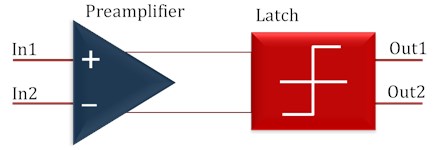
Fig. 1 shows the block diagram of Preamplifier-Latch based comparator. Note that we have used balanced-input balanced-output comparator. The synchronous triggering of SA register increases overhead time in conversion process and hence affects the speed of ADC adversely. Since the externally applied clock triggers the SA register for next step, we should think in a direction to either remove this clock completely or replace it with some alternate trigger. An effective way to vanish overhead waiting time for comparator is to generate a clock internally from comparator as soon as the comparison process is over. This totally removes the dependency of SAR ADC over the external clock to govern its functioning, thereby making it asynchronous. There should be such a comparator from which we can distinguish between a settled state and an unsettled state. The operation of the SAR logic will no longer restrained by external clock if we can design a comparator that is capable of generating a ready signal, whenever the comparator completes a comparison. A finite time will remain associated with DAC settling, but the resolving time for the comparator is no longer fixed. So, in asynchronous architecture, the DAC settling time starts immediately after the comparison is done. The time elapsed by the comparator's comparison varies from case to case. This is how the ADC can produce an output as soon as a bit is decided. This can also reduce the overhead time required for the conversion and thereby increases speed.
Fig. 1Comparator using preamplifier and latch
3. Proposed comparator
In this section Preamplifier-Latch based comparator used for Asynchronous SAR ADC design has been discussed. We have used balanced-input balanced-output comparator.
3.1. First stage: preamplifier
3.1.1. Preamplifier schematic
Preamplifier has been implemented using differential pair as shown in Fig. 2 [10]. The schematic of designed preamplifier have inputs applied at its PMOS input transistor PMOS_3 and PMOS_5. Preamplifier is used to obtain higher resolution and avoid kickback noise and also serves to overcome the offset voltage of latch that may poses hurdles for proper functioning, to be cascaded after it to make the comparator [11]. Transistors NMOS_1 and NMOS_2 are used as loads and NMOS_5 and NMOS_6 contribute in increasing output impedance and also increase the gain of the circuit. Transistor PMOS_1 and PMOS_2 make up the current mirror circuit to provide bias current for the operation. Transistor NMOS_5 is used as reset transistor. As the phase phi3 applied at the gate of NMOS_5 goes high, it will turn ON this transistor and reset the output nodes OutP and OutN to equal potential. This prevents kickback noise and reduces the probability of preamplifier giving unexpected results due to accumulation of charge at sensitive nodes.
The circuit has been implemented in 500 nm technology of Tanner S-Edit and simulated in Tanner TSpice AMIS_C5N_v4.0. The aspect ratio of each respective transistor is given in figure itself. The overall gain of preamplifier has been calculated using the formula given in Eq. (2).
From Fig. 3 we can put the values and we can mathematically calculate gain as shown in Eq. (3):
Fig. 2Preamplifier schematic
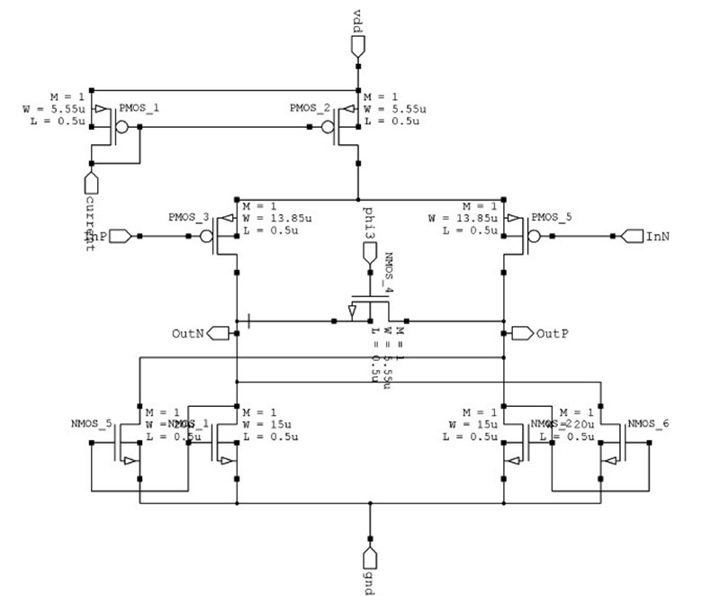
Fig. 3Gain calculation
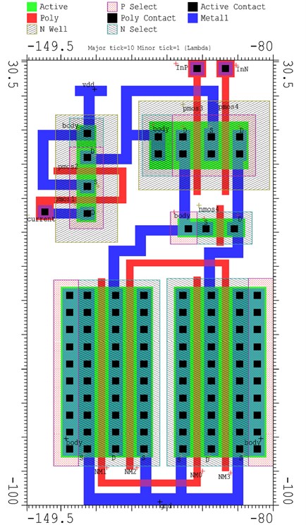
3.1.2. Preamplifier layout
The layout of preamplifier has been given in Fig. 4. The layout has been sketched in L-Edit SCN3ME_SUBM 500 nm CMOS technology. The technology node used is 500 nm and we are following rules while designing layouts and for this technology node 300 nm. A basic MOS transistor has been shown in Fig. 5 with active regions and the body to demonstrate a general layout development process.
Note that we have used poly-silicon as gate material. The advantage of using poly as gate is that it self-aligns the source and drain regions of the transistor that eases the fabrication process. A sufficient number of active contacts are distributed over the whole length to provide reliable contacts. Many technologies support a minimum size of contact and not the varying size. This is because the etch rate may vary depending upon the size so a simple and reliable solution is to distribute contacts evenly over the area [12].
In order to avoid coupling due to flow of current from drain to source in NMOS_1 and NMOS_2 pair (and NMOS_5 and NMOS_6 pair also), see schematic of preamplifier, we have taken a common drain terminal for these pairs. This reduces effects of flowing current and brings up symmetry in the design. Any gradient appearing in the microcircuit would affect them equally and hence the overall operation of preamplifier would remain more or less same [13].
Fig. 4Preamplifier layout
3.2. Second stage: positive feedback latch
3.2.1. Positive feedback latch schematic
The Latch design is comprised of two back-to-back connected inverters with their power supplies and grounds controlled by another pair of PMOS and NMOS. The schematic drawn in Tanner S-Edit has been shown in Fig. 6.
Fig. 5General MOS transistor layout
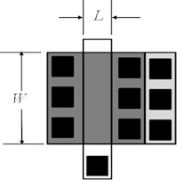
Fig. 6Latch schematic
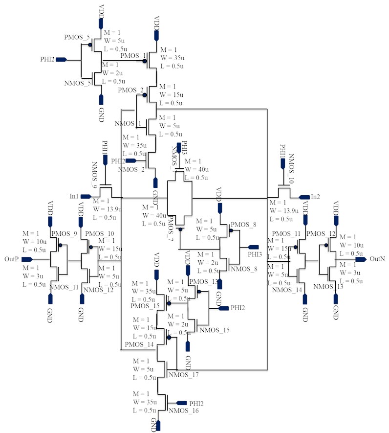
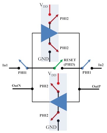
We have incorporated buffer to take output from the same line where the inputs are being applied. Inputs applied to the latch are nothing but outputs from preamplifier. To understand the working of latch, refer to Fig. 7. As the inputs are applied to latch at In1 and In2 (Fig. 7) and phase phi1 arrives at the gate of respective transistors to bring them into saturation or ON state, input is sampled and held constant at respective nodes. This phase is called sampling or tracking phase. During the phase phi2, the inverters (shown with symbols in Fig. 7) are activated as and when they get connected through power supply and hence the applied inputs are processed by latch’s back-to-back connected inverter. This processing is nothing but faithful regeneration of applied signals by repetitive positive feedback. The positive feedback results in regenerative amplification of applied inputs. This phase is called Latch phase. After successful regeneration i.e. when two signals are properly distinguished (this is possible after one time constant of latch is elapsed), phase phi3 arrives to reset the output line and make to reach them at same voltage level. The purpose of phase phi3 is to bring both output nodes at the same potential. This will reduce differential voltage at both the nodes and hence makes the latch ready for next step of comparison.
Note that all the three phases used in latch design as non-overlapping, with their time periods chosen as to provide sufficient time for respective phases to complete their assigned objectives.
Fig. 7General block diagram of latch
3.2.2. Positive feedback latch layout
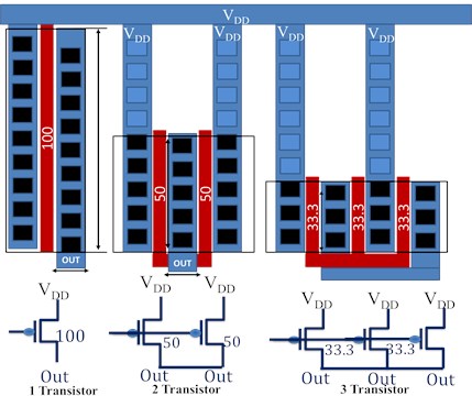
The Layout of latch has been shown in Fig. 8. The simplest type of transistor is shown in Fig. 5 but for the case of larger transistors (those with aspect ratio > 10); they cannot be simply drawn like the former. They need special attention as they may cause significant problems if not handled carefully. Their size is therefore molded to some manageable shape by “fingering” which involves dividing the W of transistor into multiple identical sections. This saves area and makes transistor easy to handle without changing its aspect ratio. Further, we can merge or share source-drain regions between two suitable combinations and this will result in reduction of parasitic junction capacitance to nearly half [14]. An example is shown in Fig. 9 that demonstrate the whole process of managing the size of longer transistors. The preamplifier and latch already discussed are the two elements that constitute the comparator Fig. 1. The outputs of preamplifier (Fig. 2) are simply applied to inputs of latch (Fig. 6) and the outputs of latch serve as outputs of comparator. Note that phase phi3 is common to both preamplifier as well as latch, making the whole design of comparator highly reluctant towards differential noise.
Fig. 8Latch layout
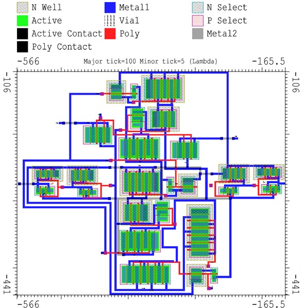
Fig. 9Transistor fingering
4. Simulation result of comparator
The simulation was carried out on a system having Microsoft® Windows 10™ Operating System- with Intel® Core™ 2 Duo, 2.00 GHz with 4 GB RAM; additionally a video card with 256 MB of dedicated memory having1280×1024 Resolution - True Color (24-bit) using Tanner EDA. This integrated front-end tool suite includes S-Edit for schematic capture and netlist generation, T-Spice for circuit simulation by using netlist obtained from S-Edit and W-Edit for waveform viewing and analysis.
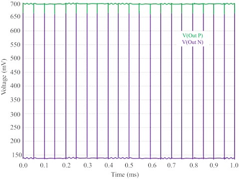
Fig. 10 shows the transient response of Preamplifier-Latch based Comparator when one of the inputs is subjected to a time varying ramp signal and another one keep at a constant voltage. Note that our comparator has two inputs as well as two outputs, making it balanced-input balanced-output in nature. Two inputs namely, InN and InP are regarded as negative and positive terminals of comparator. Output pins called OutP and OutN are positive and negative outputs. As the positive/negative input is applied HIGH, so output OutP/OutN will go HIGH.
In order to judge the correct working of comparator, one of the input is given a constant voltage while other input is varied in the form of ramp voltage. We can see from the figure that when inp > inn then outp > outn and vice-versa.
Fig. 10Comparator transient analysis
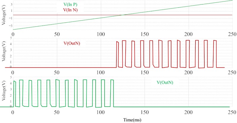
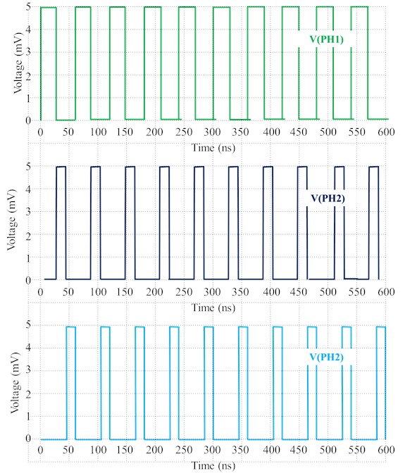
Fig. 11 presents the transient response of phases of comparator. Note that all three phases are non-overlapping namely phi1 phi2 and phi3. When the sampling phase phi1 arrives, the input present at these terminals of latch is sampled. When this phase ends and the tracking phase phi2 arrives, the input values now undergo regenerative amplification due to positive feedback present in latch and after sufficient amount of time this step of tracking phase ends at the falling edge of phase phi2. Now in reset phase phi3 the two output lines are brought to same potential in order to make latch ready for next cycle [15].
Table 1 represents the comparison of power consumption of previously reported latch with this work. Even though the proposed work is done on 500 nm CMOS Technology, which is comparatively higher than other used technologies, still it dissipates 65 μW power, which is significantly less when compared with other related comparator design technologies [16].
Table 1Comparison of power consumption
Parameters | Ref [17] | Ref [18] | Ref [19] | Ref [20] | Proposed work |
Technology (nm) | 35 | 35 | 35 | 35 | 500 |
Supply (V) | 3.3 | 3.3 | 3.3 | 3.3 | 1 |
Power consumption (μW) | 3300 | 600 | 2000 | 1000 | 65 |
Table 2Comparison of speed
Parameters | Ref [21] | Ref [22] | Ref [23] | Ref [24] | Proposed work |
Technology (nm) | 65 | 180 | 90 | 180 | 500 |
Speed (KSP) | 20 | 100 | 500 | 200 | 2100 |
Table 2 represents the comparison of speed of the ADCs having other comparators with ADC having the proposed comparator. This data is taken from a popular ADC survey conducted by B. Murman. The survey includes some of the important SAR ADC designs.
Fig. 11Non-Overlapping Phases (phi1, phi2 and phi3) of positive feedback latch
5. Conclusions
In the proposed work we have successfully represented the design of a high speed compact and low power, Balanced-Input Balanced-Output Preamplifier Latch based Comparator using 500 nm CMOS Technology. A unique concept of making Comparator specifically for Asynchronous SAR ADC, that will help in achieving the asynchronous operation and hence reduce the overhead time, has been successfully presented. We have implemented the proposed design in 500 nm technology and managed to reduced power to 65 μW. Further the proposed comparator is capable of increasing the speed of overall ADC. We have also compared our design with other contemporary designs that justifies the good performance of circuit. Still there is a huge scope to further improve the speed of operation if we can manage to implement Time-Interleaving. Another way for further increasing the speed is to implement the comparator using BiCMOS technology which is likely to impart low output impedance, high gain as well as speed to overall design.
References
-
Zhu Yan, et al. A 10-bit 100-MS/s reference-free SAR ADC in 90 nm CMOS. IEEE Journal of Solid-State Circuits, Vol. 45, Issue 6, 2010, p. 1111-1121.
-
Liu Chun Cheng, et al. A 10-bit 50-MS/s SAR ADC with a monotonic capacitor switching procedure. IEEE Journal of Solid-State Circuits, Vol. 45, Issue 4, 2010, p. 731-740.
-
Tai Hung Yen, et al. A 0.004 mm 2 single-channel 6-bit 1.25 GS/s SAR ADC in 40nm CMOS. IEEE Asian Solid-State Circuits Conference (A-SSCC), 2013.
-
Jeon Heungjun, Kim Yong Bin A novel low-power, low-offset, and high-speed CMOS dynamic latched comparator. Analog Integrated Circuits and Signal Processing, Vol. 70, Issue 3, 2012, p. 337-346.
-
Schinkel Daniel, et al. A double-tail latch-type voltage sense amplifier with 18ps setup+ hold time. IEEE International Solid-State Circuits Conference, 2007.
-
Kandpal Kavindra, Saloni Varshney, Manish Goswami A high Speed-Low power comparator with composite cascode pre amplification for oversampled ADCs. Journal of Automation and Control, Vol. 1, Issue 14, 2013, p. 301-305.
-
Miyahara Masaya, et al. A low-noise self-calibrating dynamic comparator for high-speed ADCs. IEEE Asian Solid-State Circuits Conference, 2008.
-
Wang Riyan, et al. A high-speed high-resolution latch comparator for pipeline analog-to-digital converters. International Workshop on Anti-Counterfeiting, Security and Identification (ASID), 2007.
-
Tseng Wei Hsin, et al. A 12-bit 104 MS/s SAR ADC in 28 nm CMOS for digitally-assisted wireless transmitters. IEEE Journal of Solid-State Circuits, Vol. 51, Issue 10, 2016, p. 2222-2231.
-
Tabassum Shabi, Anush Bekal, Manish Goswami A low power preamplifier latch based comparator using 180nm CMOS technology. IEEE Asia Pacific Conference on Postgraduate Research in Microelectronics and Electronics (PrimeAsia), 2013.
-
Johns David A., Ken Martin Analog Integrated Circuit Design. John Wiley and Sons, 2008.
-
Hastings A. The Art of Analog Layout. 2nd Ed., Prentice Hall, 2006.
-
Sharma Ashutosh, Mohd Dilshad Ansari, Rajiv Kumar A comparative study of edge detectors in digital image processing. 4th International Conference on Signal Processing, Computing and Control (ISPCC), 2017.
-
Sharma Ashutosh, Rajiv Kumar Realistic comparison of performance parameters of static and dynamic unicast routing over mesh topology. International Journal of Scientific and Engineering Research, Vol. 6, Issue 12, 2015, p. 202-207.
-
Rathee Geetanjali, et al. A trust management scheme to secure mobile information centric networks. Computer Communications, Vol. 151, 2020, p. 66-75.
-
Poongodi M., et al. Prediction of the price of Ethereum blockchain cryptocurrency in an industrial finance system. Computers and Electrical Engineering, Vol. 81, 2020, p. 106527.
-
Wong Yanyi Liu, Marc Cohen H., Pamela Abshire A. A 1.2-GHz comparator with adaptable offset in 0.35-μm CMOS. IEEE Transactions on Circuits and Systems I: Regular Papers, Vol. 55, Issue 9, 2008, p. 2584-2594.
-
Kazeminia Sarang, et al. A 500 MS/s 600 µW 300 µm 2 single-stage gain-improved and kickback noise rejected comparator in 0.35 µm 3.3 v CMOS Process. IEICE Transactions on Electronics, Vol. 94, Issue 4, 2011, p. 635-640.
-
Sheikhaei Samad, Shahriar Mirabbasi, Andre Ivanov A 0.35/spl mu/m cmos comparator circuit for high-speed ADC applications. IEEE International Symposium on Circuits and Systems, 2005.
-
Baradaranrezaeii Ali, et al. A 1GS/s low-power low-kickback noise comparator in CMOS process. 20th European Conference on Circuit Theory and Design (ECCTD), 2011.
-
Yip Marcus, Chandrakasan Anantha P. A resolution-reconfigurable 5-to-10b 0.4-to-1V power scalable SAR ADC. IEEE International Solid-State Circuits Conference, 2011.
-
Verma Naveen, Chandrakasan Anantha P. A 25μW 100kS/s 12b ADC for wireless micro-sensor applications. IEEE International Solid-State Circuits Conference, 2006.
-
Liou Chang Yuan, Hsieh Chih Cheng A 2.4-to-5.2 fJ/conversion-step 10b 0.5-to-4MS/s SAR ADC with charge-average switching DAC in 90nm CMOS. IEEE International Solid-State Circuits Conference Digest of Technical Papers, 2013.
-
Han Dong, et al. A 0.45 V 100-Channel Neural-Recording IC With Sub-$\mu {\rm W} $/Channel Consumption in 0.18$\mu {\rm m} $ CMOS. IEEE Transactions on Biomedical Circuits and Systems Vol. 7, Issue 6, 2013, p. 735-746.
About this article

