Abstract
Inverters are basically power electronics devices that are used to convert DC power to AC at a required frequency and voltage level. Their main application area in real-time is in high voltage and high-power applications in which the switching stress as well as total harmonic distortion must be low. Multilevel inverter technology has been emerging in recent times, as a very important substitute in for high-power medium-voltage energy governed devices. Multi-level inverters also have a major role in interconnected grid systems used nowadays. There are several major topologies of multilevel inverters that exist in literature: Diode clamped (DMLI) (aka neutral-point clamped), and Flying capacitor multilevel inverter (FCMLI) (aka capacitor-clamped) [1] and Cascaded H-bridges converter (CMLI) (i.e., cascaded multicell using separate dc sources). This paper discusses the principal benefits and drawbacks of increasing the number of levels of the inverter and how it has an effect on the efficiency and losses in the MLI architecture and how this difficulty as well as the overall performance of the systems can be improved using a novel Bridged-Cascaded H-bridge MLI topology. There are n-level inverter topologies possible. The paper proposes a novel bridged-insert cascaded MLI topology. The focus of the paper is on 5-level inverter topologies. The simulation has been carried out using MATLAB/Simulink.
Highlights
- The multilevel inverters can be functioned both at its fundamental switching frequency as well as the high switching frequency PWM.
- Obtain input current with comparatively much lower distortion.
- Generate smaller common-mode (CM) voltage.
- Reduces the stress in the motor bearings.
- We can completely eliminate the CM voltage by using sophisticate d modulation techniques.
- Reduces the harmonic components present in the waveform
1. Introduction
With advancements in technology, the demand for high power devices is on the rise. The power requirement these days are in the megawatt level. It is not possible nowadays to connect a single power semiconductor switch directly to a medium-voltage grid. The medium voltage grid has voltage ratings as follows: 2.3, 3.3, 4.16, or 6.9 kV. In order to overcome this problem, multilevel inverters have been invented [2]. Power electronics involves the controlling and conditioning of electric power. The electric power maybe AC or DC power of given amplitude. Electric power conversion becomes necessary when the power handling capability of the load is different from what is actually available (at the input side or source end). The conversion is primarily done using switches-including semiconductor devices such as diodes, thyristors, IGBT’s, MOSFETs, etc. [3, 4]. Multilevel inverters are power electronic devices used to synthesize a required output voltage level from several input dc inputs voltage levels. Multilevel inverters consist of an array of power semiconductor devices and other active elements such as capacitor. The commutation of the switches adds to the capacitor voltages. The power semiconductors however can withstand only reduced voltages. Compared to conventional two-level inverter topologies, the multilevel inverter architectures provide a medium to high voltage range. Multilevel inverters provide enhanced voltage and current waveforms and also have the capability to reduce the unwanted harmonics. Multilevel inverters help diminish the switching losses. Their outputs yield multi-step voltage which helps to achieve improved power quality as well as better voltage capability. Of this, the most attractive feature is the small voltage step size of the multilevel inverters – it helps in achieving high voltage capability, lower harmonic components, lower switching losses, better electromagnetic compatibility, and improved power quality. The multilevel inverter can be functioned in both its fundamental as well as high switching frequencies [5].
The following are the advantages of multilevel inverter architecture:
1) It is the smaller output voltage step of multilevel inverters that is the main attractive features:
a) Increases the voltage capability,
b) Reduces the harmonic components present in the waveform,
c) Reduces the switching losses,
d) Improves the electromagnetic compatibility.
e) Generate output voltages with extremely low distortion and lower /.
2) Besides, the multilevel inverters can be functioned both at its fundamental switching frequency as well as the high switching frequency PWM.
3) They obtain input current with comparatively much lower distortion.
4) They generate smaller common-mode (CM) voltage. This helps reduce the stress in the motor bearings. However, we can completely eliminate the CM voltage by using sophisticate d modulation techniques.
Besides the various advantages presented by a multilevel inverter, it also comes at the cost of a few disadvantages:
1) The most notable drawback is that the power semiconductor switches require multilevel power conversion.
2) The small voltage steps are typically produced by isolated voltage sources or a bank of series capacitors. As for the isolated voltage sources their availability may be a major concern and the next problem is the voltage balance requirement of the series capacitor network.
2. Literature survey
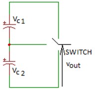
Fig. 1, 2 and 3 depict one phase leg of inverters with different 2 levels, 3 levels and levels, respectively. An ideal switch can be used to represent a semiconductor device with number of positions. The 2-level inverter generates an output voltage with two values with respect to the negative terminal of the capacitor, hence the name. Similarly, a 3-level inverter generates three voltages, and an -level, voltage values.
Fig. 1Single-phase inverter with different 2 levels
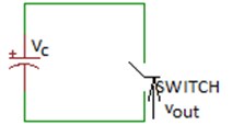
Fig. 2Single-phase inverter with different 3 levels
By varying the number of levels in the inverter, the output voltage will show varying number of steps. So, as the number of levels increase, the number of steps in the waveform will also correspondingly increase; it therefore reduces the harmonic distortion. But, on the other hand, as the number of levels is increased it leads to a rise in the complexity of the topology and also presents voltage imbalances.
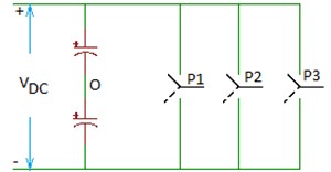
Fig. 4 depicts a three-phase voltage source inverter, also known as a two-level inverter. P1, P2, and P3 are the poles and is the neutral point.
The poles are connected to loads and these loads are considered to be inductive. The current through an inductive circuit should never be open. So, a path should always be provided for the current to flow through. So, one of the ends of the pole is connected to the load terminal, whereas the other end will be connected to one throw or the other. Hence, a path will always be present for the current to pass through. Power can flow in both the directions. The switches can be depicted by IGBTs. We are using two IGBTs in a single leg. A single unit or switch is able to conduct current in both the directions. When one of the switches in a leg is on, the other is blocked or in OFF state [1, 6, 7].
Fig. 3Single-phase inverter with different n levels
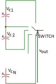
Fig. 43-phase voltage-source inverter
2.1. Realization of different types of switches
2.1.1. SPDT Switch or a simple 2-level inverter realization
The internal realization of simple SPDT switch using IGBTs and diodes is shown in Fig. 5 below. represents the pole and T1 and T2, the throws. The voltage across the two throws is +. One end of the pole will be connected to one of the throws (T1 or T2), and the other end to the load. Depending on the direction in which the load current is flowing through the switch, it is either the diode or the transistor that forms a component part of the switch that will be conducting. So, the diode and the transistor form a complementary pair (either S1and D2 are ON or D1 and S2 are ON). The circuit therefore operates as a SPDT switch. There are only two possible output voltage levels at the pole end: + or –. So, this circuit can be used a 2-level inverter as well.
Fig. 5SPDT switch electronic realization
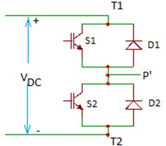
2.1.2. SPTT Switch or a simple 3-level inverter realization.
Fig. 6 depicts the electronic realization of Single Pole Triple Throw (SPTT) switch. It is observed that the waveform quality of such an SPTT switch is superior to that of a SPDT switch.
Case 1: In order to connect to T1, S1 and S2 must be ON.
Case 2: In order to connect to T2, S2 and S3 must be ON.
Case 3: In order to connect to T3, S3 and S4 must be ON.
The waveform quality of an SPTT switch is attributed due to the following reason. The average pole voltage at at any point will be the average of the voltages at T1, T2 and T3. If T1 is at +0.5, T3 at –0.5and T2 at 0 V, then is between +0.5 and –0.5. If we want to obtain a pole voltage of 0.25, we can realize it using a 2-level inverter. It can be obtained by applying +0.5 for a longer time and –0.5 for a relatively shorter time, so that the average of the voltage applied approximates to a 0.25. However, the same realization can be done using a 3-level inverter as follows. A 3-level inverter, as the name suggests, can produce 3 output voltage levels: ±0.5 and 0. So, simply apply +0.5 and 0 V for the same amounts of time. This second method is much more efficient and generates a waveform of better quality than that produced using a 2-level inverter, since it is a time-averaging technique and it ensures that the maximum instantaneous error possible. Yet another advantage of this method is that the diodes D1 and D2 keep a constant check to ensure that the switches only work between the specified voltage ranges.
Fig. 6SPTT switch electronic realization
2.2. Types of multilevel inverters
There are several major topologies of multilevel inverters that exist in literature; the classification is based on the different mechanisms involved. This paper discusses the types of symmetrical MLIs.
Fig. 7The categories of multilevel inverters
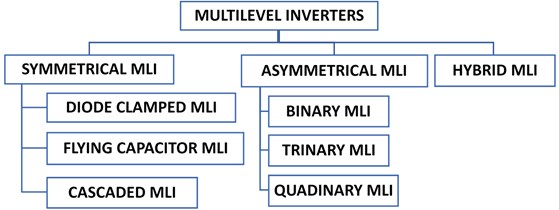
2.2.1. Symmetrical multilevel inverters
These inverters have equal amplitude of voltage sources. Diode clamped (DMLI or neutral-point clamped), flying capacitor multilevel inverter (FCMLI or capacitor-clamped) and Cascaded H-bridges converter (CMLI) (i.e., cascaded multicell using separate dc sources) are the types of symmetrical multilevel inverters.
H-bridge design was the first topology to be developed. In this, the scaling can be done easily. The H-bridge inverter consists of isolation transformers for isolating the voltage source. Then the diode-clamped inverter was developed. It consisted of a of a series capacitors. Later came the flying-capacitor topology. The difference compared to the diode-clamped inverter is that in flying-capacitor topology the voltage levels are clamped using floating capacitors.
2.2.1.1. Diode clamped or neutral-point clamped (NPC) multilevel inverter
This inverter mainly uses diodes to limit voltage stress on the power device. Assume that the voltage across each capacitor and each switch is . An m level inverter consists of (m-1) voltage sources, (m-1) capacitors, 2(m-1) switching devices and (m-1)×(m-2) diodes per leg [8, 9].
Single-phase Three-level NPC Inverter
Case 1: To connect the pole to T1, S1 and S2 are ON, whereas S3 and S4 are OFF.
Case 2: To connect the pole to T2, S2 and S3 are ON, whereas S1 and S4 are OFF.
Case 3: To connect the pole to T3, S3 and S4 are ON, whereas S1 and S2 are OFF or S1 and S2 are ON, whereas S3 and S4 are OFF.
So, on analysing, we can conclude that S1 and S3 are complementary and so are S2 and S4. So, we can see that S2 and S3 tend to ON longer than the switches S1 and S4, and consecutively dissipate more power than S1 and S4. So, the losses from S2 and S3 are higher than the losses from S1 and S4. So, we need two different gating signals one for S1 and S3, and another for S2 and S4 (since these pairs are complementary during operation). So, comparison we find that a 2-level inverter requires only a single gating signal, whereas a 3-level inverter requires 2 gating signals.
Fig. 8One leg of a 3-level NPC inverter
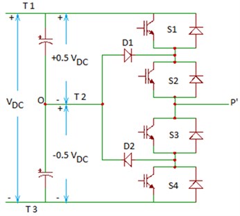
Fig. 95-level flying capacitor clamped MLI
2.2.1.2. Flying capacitor multilevel inverter
This inverter mainly uses capacitors to limit voltage stress on the power device. The circuit diagram is very similar to the diode clamped multilevel inverter, with the only difference that capacitors are used to divide the input DC voltage, so that the voltage across each of the capacitors as well as each switch is . For an m-level inverter, (m-1) capacitors are required. The diodes of the diode-clamped MLI are replaced by capacitors. However, at the input end, the 2 capacitors will be pre-charged to a fixed voltage level in order to act as the DC voltage source, whereas, the other two capacitors will not be connected to any fixed voltage- in other words it is varying and hence the name ‘flying’. The Fig. 9 shows the 5-level flying capacitor clamped MLI [10].
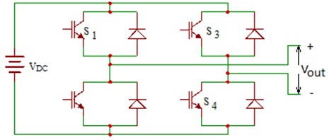
2.2.1.3. Conventional cascaded multilevel inverter
This type of inverter is based on H-bridge inverters they are connected together in series. The output voltage will be sinusoidal in nature. It is calculated as the sum of the voltages produced by each of the cells. If n is the number of cells, then there will be (2+1) output voltage levels. The main plus point of the cascaded MLI is that it uses lesses number of component devices compared to the other two types of symmetrical MLIs. Thereby, the price as well as the weight of the cascaded MLI is comparatively much less than the other two types of MLI topologies [11, 12].
2.2.2. Single-phase cascaded 3-level inverter realization
Fig. 10 depicts a cascaded inverter with multiple levels.
For switch , the transistor is represented as and the diode as . The working of the circuit is as follows:
Case 1: Applying the gating signal, if switch S1 is ON, transistor Q1 and Q4 will be ON or diodes D2 and D3 will be ON. Then the output is +.
Case 2: If S2 is ON, Q2 and Q3 will be ON or D1 and D4 will be ON. The output is –.
Case 3: However, if S3 is ON, then either Q1 or D3 will be ON, or D1 and Q3 will be ON. In either case the output will be 0 V.
Case 4: Similarly, if S4 is ON, then either Q2 or D4 will be ON, or D2 and Q4 will be ON. In either case the output will be 0 V.
Fig. 10Conventional cascaded 3-level MLI realization
2.3. Five-level mli
In a 2-level inverter, the output voltage can have only 2 voltage levels. A 3-level inverter in the other hand can have ±/2, 0 (3 values). This section observes how the output voltage value changes for a 4-level and 5-level MLI [13, 14].
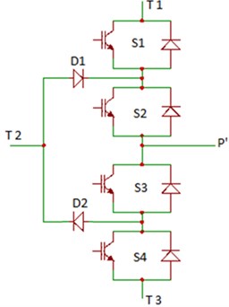
The circuit shown in Fig. 11 is that of a single pole four throw switch which consists of one pole and 4 throws.
The pole voltage can take values: ±0.5, ±0.167.
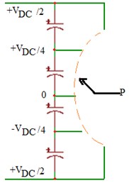
The Fig. 12 depicts a single pole five throw switch.
The pole voltage can take values: ±0.5, ±0.25, 0.
2.3.1. Single-phase five-level NPC inverter
2.3.1.1. Diode-clamped inverter
Initially, to start with, let us consider a 5-level diode-clamped inverter. Take one leg first. The dc rail 0 is the reference point of the output phase voltage. The steps to obtain the 5-level waveform are:
Case 1: For an output voltage level , turn on all upper-half switches S1 through S4.
Case 2: For an output voltage level /2, turn on two upper switches S3 through S4 and two lower switches S1’ and S2’.
Case 3: For an output voltage level 0, turn on all lower half switches S1’ through S4’.
Fig. 11Single pole four throw switch
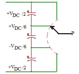
Fig. 12Single pole five throw switch
State 1 is known as ON condition whereas State 0 is known as OFF condition. Each switch is turned ON only for one-unit time per cycle. The architecture in Fig. 5 consists of four complementary switch pairs in each phase.
The switch-pairs forming the inverter legs are (S1, S1’), (S2, S2’), (S3, S3’) and (S4, S4’). Therefore, if any one of the switches in the complementary pairs is ON, the other switch of the same pair must be OFF. The line voltage consists of the positive phase-leg voltage of terminal and the negative phase-leg voltage of terminal. Each phase-leg voltage tracks one-half of the sinusoidal waves. So, the resulting line voltage is a five-level staircase wave (refer Table 1).
Fig. 13Diode-clamped multilevel inverter with 5-levels
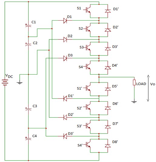
Table 1Diode clamped inverter-switch states and output voltage levels
Switch state | Output | |||||||
S1 | S2 | S3 | S4 | S1’ | S2’ | S3’ | S4’ | |
ON | ON | ON | ON | OFF | OFF | OFF | OFF | +/2 |
OFF | ON | ON | ON | ON | OFF | OFF | OFF | +/4 |
OFF | OFF | ON | ON | ON | ON | OFF | OFF | 0 |
OFF | OFF | OFF | ON | ON | ON | ON | OFF | –/4 |
OFF | OFF | OFF | OFF | ON | ON | ON | ON | –/2 |
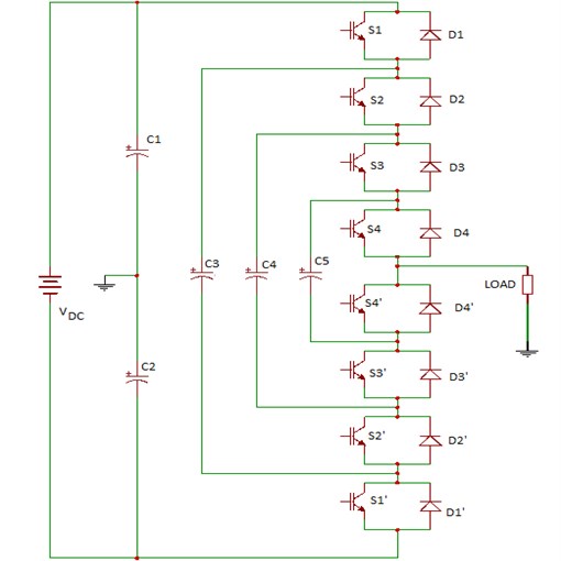
2.3.1.2. Flying capacitor-clamped inverter
Fig. 14 shows the flying capacitors based multilevel inverter topology.
Fig. 14Flying capacitor multilevel inverter with 5-levels
2.3.1.3. Single-phase cascaded 5-level inverter realization
Fig. 15Cascaded multilevel inverter with 5-levels
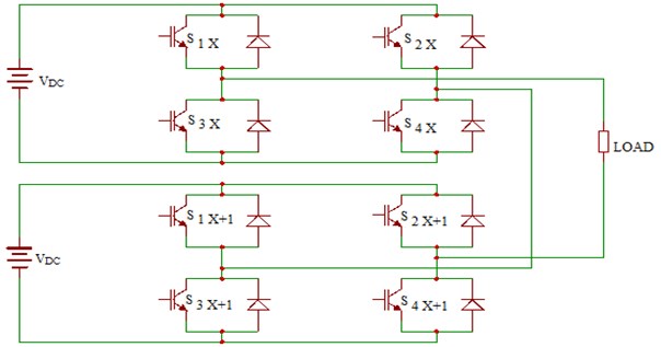
Table 2Flying capacitor inverter-switch states and output voltage levels
Switch state | Capacitor state | Output | |||||
S1 | S2 | S3 | S4 | C3’ | C4’ | C5’ | +/2 |
ON | ON | ON | ON | Not charging | Not charging | Not charging | +/4 |
ON | ON | ON | OFF | Not charging | Not charging | + | |
ON | ON | OFF | ON | Not charging | + | – | |
ON | OFF | ON | ON | + | – | Not charging | |
OFF | ON | ON | ON | – | Not charging | Not charging | |
OFF | OFF | ON | ON | Not charging | – | Not charging | 0 |
OFF | ON | OFF | ON | – | + | – | |
OFF | ON | ON | OFF | – | Not charging | + | |
ON | OFF | OFF | ON | + | Not charging | – | |
ON | OFF | ON | OFF | + | – | + | |
ON | ON | OFF | OFF | Not charging | + | Not charging | |
ON | OFF | OFF | OFF | + | Not charging | Not charging | –/4 |
OFF | ON | OFF | OFF | – | + | Not charging | |
OFF | OFF | ON | OFF | Not charging | – | + | |
OFF | OFF | OFF | ON | Not charging | Not charging | – | |
OFF | OFF | OFF | OFF | Not charging | Not charging | Not charging | –/2 |
3. Significance of the number of levels in a multilevel inverter
3.1. Losses in 2-level inverter
The 3-phase Voltage-source inverter in Fig. 4 has been represented in its electronic realization in the Fig. 16.
Here the losses in all the 3 legs are equal since it is a balanced load condition that we are considering. That implies that the losses due to bottom and top devices are the same. The losses include both the conduction and the switching losses. If PWM techniques are applied, however, this balance load condition may get varied and hence may lead to unequal losses in each leg.
Table 3Switch states and voltage levels of five level cascaded inverter
Switch state | Output () | |||
ON | OFF | ON | OFF | +2 |
ON | OFF | OFF | OFF | + |
ON | OFF | ON | ON | + |
OFF | OFF | ON | OFF | + |
ON | ON | ON | OFF | + |
OFF | OFF | OFF | OFF | 0 |
ON | ON | ON | ON | 0 |
ON | OFF | OFF | ON | 0 |
OFF | ON | ON | OFF | 0 |
OFF | OFF | ON | ON | 0 |
ON | ON | OFF | OFF | 0 |
OFF | ON | ON | ON | – |
OFF | ON | OFF | OFF | – |
ON | ON | OFF | ON | – |
OFF | OFF | OFF | ON | – |
OFF | ON | OFF | ON | –2 |
3.2. Losses in 3-level inverters
This is not the same case in multilevel inverters with 3 or more levels – the working is different. Consider Fig. 10. As we said there that since switches S2 and S3 are ON for more time than S1 or S4, the power dissipation is higher in that case. That means in turn that the conduction losses are also higher in S2 and S3. Rather, the middle two devices suffer more losses.
Fig. 162-level voltage source inverter
4. Proposed method
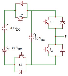
Considering the main disadvantage of the Cascaded MLI topologies, we find that the number of switches used for the circuit are much higher and hence account for a higher loss. Correspondingly even the harmonic distortion will be much higher. To overcome this problem, this paper proposes a bridged-insert cascaded MLI topology. A 5-level MLI of this type is shown in Fig. 17.
Fig. 17Bridged-insert cascaded 5-level MLI
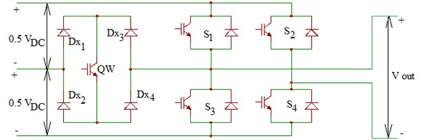
As you can see, the number of switches has been reduced by 3 and hence the loss can also be reduced. The working can be understood in the Table 4 that explain the devices that are ON and OFF and the corresponding output voltages.
Table 4Switch states and voltage levels of five level proposed inverter
Switch states | Output | ||||
S1 | S2 | S3 | S4 | QW | |
ON | OFF | OFF | ON | OFF | |
OFF | OFF | OFF | ON | ON | /2 |
OFF | OFF | ON | ON | OFF | 0 |
OFF | ON | OFF | OFF | ON | –/2 |
OFF | ON | ON | OFF | OFF | – |
5. Results
The study and analysis of the diode clamped 5-level inverter, flying capacitor-clamped 5-level inverter, cascaded 5-level inverter as well as the proposed bridged-insert cascaded 5-level inverter were carried out using MATLAB/Simulink Tool.
The voltage output obtained across the load or in other words, at the pole was analyzed and compared. Not only that, the FFT (Fast Fourier Transform) analysis was also done in order to analyze the harmonic distortion present in the output.
5.1. Diode clamped MLI
Fig. 18The output voltage waveform of the 5-level diode-clamped MLI
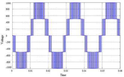
Fig. 19The FFT of the 5-level diode-clamped MLI. Fundamental (50 Hz) = 38.7 Hz, THD = 21.97 %
5.2. Flying-capacitor clamped MLI
Fig. 20The output voltage waveform of the 5-level flying capacitor clamped MLI
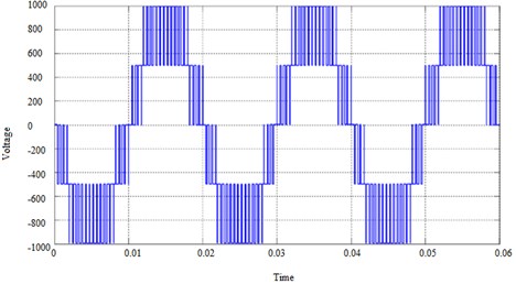
Fig. 21The FFT of the 5-level flying capacitor clamped MLI. Fundamental (50 Hz) = 967.4 Hz, THD = 39.92 %
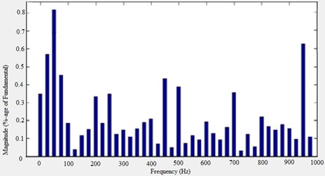
5.3. Conventional cascaded MLI
Fig. 22The output voltage waveform of the 5-level conventional cascaded MLI
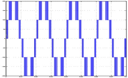
Fig. 23The FFT of the 5-level cascaded MLI. Fundamental (50 Hz) = 278.6 Hz, THD = 20.93 %
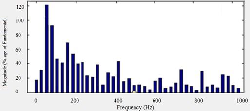
5.4. Proposed novel bridged-insert cascaded MLI
Fig. 24The output voltage waveform of the 5-level bridged-insert cascaded MLI
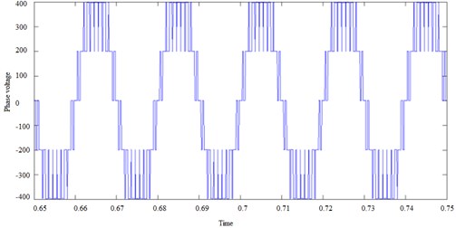
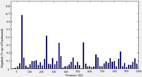
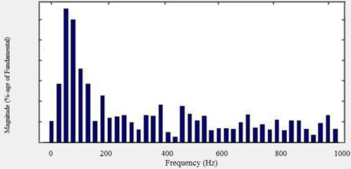
Fig. 25The FFT of the 5-level bridged-insert cascaded MLI. Fundamental (50 Hz) = 120 Hz, THD = 26.78 %
6. Analysis and comparison
Depending on the result obtained from the study conducted, a comparative analysis can be carried out. The above discussed types of MLI topologies are compared in a tabular format as shown below in Table 5.
Table 5Comparison
Type of MLI | Advantage | Disadvantage |
Diode clamped multilevel inverter | 1. High efficiency 2. No need of filters for reducing harmonics 3. Reactive power flow can be altered 4. The control method is very simple | 1.For high levels, more number of diodes are required 2. Real power flow control for individual converter is difficult |
Flying capacitor multilevel inverter | 1. Phase redundancies are available for balancing the voltage levels of the capacitors 2. The flow of Real and reactive power can be controlled 3. The large number of capacitors enables the inverter to ride through short duration outages and deep voltage sags | 1. Control is complicated to track the voltage levels for all of the capacitors. Also, recharging all of the capacitors to the same voltage level is complex 2. Switching utilization and efficiency are poor for real power transmission 3. The large numbers of capacitors are both more expensive and bulky than clamping diodes in multilevel diode-clamped converters. Packaging is also more difficult in inverters with a high number of levels |
Cascaded multilevel inverter | 1. The number of possible output voltage levels is more than twice the number of dc sources ( 2s +1) 2. The series of H-bridges makes for modularized layout and packaging. This will enable the manufacturing process to be done more quickly and cheaply | 1. Separate DC sources are required for the real power conversion |
Bridged half-cascaded MLI | 1. Lesser number of switches 2. Reduce harmonic distortion 3. Reduces area | 1. Number of gate signals could be increased |
7. Conclusions
Depending the comparative study made of the 3 types of symmetrical MLIs, it can be seen that the cascaded multilevel inverter requires minimum number of components when compared will other types, which thereby reduces the weight, price and size of the inverter device. With fewer switches or on-board components, the complexity of the circuit also reduces. So, it can be concluded that the cascaded inverter is the better choice. However, if we are able to reduce the number of switches even further, the losses and harmonic distortions can be further reduced. Hence, the novel topology of bridge-insert cascaded MLI was proposed. It used only 5 switches compared to the 8 switched used in the conventional cascaded MLIs, hence making the losses diminished. From the FFT analysis, it is found the harmonic distortions are also much reduced compared to the other inverter topologies. Hence the proposed technique of bridge-insert cascaded MLI is the best.
References
-
Sayed Mahmoud A., Mahrous Ahmed, Elsheikh Maha G., Orabi Mohamed PWM control techniques for single-phase multilevel inverter based controlled DC cells. Journal of Power Electronics, Vol. 16, Issue 2, 2016, p. 498-511.
-
Rodríguez José, Lai Jih Sheng, Peng Fang Zheng Multilevel inverters: a survey of topologies, controls, and applications. IEEE Transactions on Industrial Electronics, Vol. 49, Issue 4, 2002, p. 724-738.
-
Kou Xiaomin, Corzine Keith A., Familiant Yakov L. Full binary combination schema for floating voltage source multilevel inverters. IEEE Transactions on Power Electronics, Vol. 17, Issue 6, 2002, p. 891-897.
-
Chattoraj Juhi, Dwivedi Arpan, Pahariya Yogesh Study of multilevel inverters for rural electrification using renewable saps system. International Journal of Engineering Sciences and Management, Vol. 7, Issue 1, 2017, p. 102-106.
-
Hariprasadhsingh S., Raju P., Zabiullah S. Systematic design of hybrid cascaded multilevel inverters with simplified DC power supply and low switching losses. International Journal of Engineering Inventions, Vol. 3, Issue 4, 2013, p. 32-50.
-
Vijaybabu S., Kumar Naveen A., Krishna Rama A. Reducing switching losses in cascaded multilevel inverters using hybrid-modulation techniques. International Journal of Engineering Science Invention, Vol. 2, Issue 4, 2013, p. 26-36.
-
Suresh Sanju K., Viswanathan M. P. A novel method to improve the control performance of multilevel inverter by multisampling. IOSR Journal of Electrical and Electronics Engineering (IOSR-JEEE), Vol. 5, Issue 5, 2013, p. 6-11.
-
Kumar Vinod P., Kumar Ch. Santosh, Reddy Ramesh K. single phase cascaded multilevel inverter using multicarrier PWM technique. ARPN Journal of Engineering and Applied Sciences, Vol. 8, Issue 10, 2013, p. 796-799.
-
Gunaraj Cornelius P. Multi sampled multilevel inverters to improve control performance. IJREAT International Journal of Research in Engineering and Advanced Technology, Vol. 1, Issue 1, 2013, p. 1-6.
-
Balamurugan C. R., Natarajan S. P., Arumugam M. A review on various multilevel inverter topologies. Global Journal of Advanced Research, Vol. 2, Issue 1, 2015, p. 142-153.
-
Stala Robert Natural capacitor voltage balance in multilevel flying capacitor converters – a review of research achievements. Power Electronics and Drives, Vol. 36, Issues 2, 2016, p. 5-33.
-
Leon Jose I., Franquelo Leopoldo G., Kouro Samir, Wu Bin, Vazquez Sergio Novel modulator for the hybrid two-cell flying-capacitor based ANPC converter. International Conference on Power Engineering, Energy and Electrical Drives, 2011.
-
Naderi Roozbeh, Smedley Keyue A new hybrid active neutral point clamped flying capacitor multilevel inverter. IEEE Applied Power Electronics Conference and Exposition, 2015.
-
Raju Athira, Arun S. Hybrid multilevel inverter topology with an independent control for photovoltaic system. International Journal of Advanced Research in Electrical, Electronics and Instrumentation Engineering, Vol. 2, Issue 1, 2013, p. 278-287.
About this article

