Abstract
The characteristics of vibrations in microbolometer had significant impact on the performances of its infrared absorption. Due to the complex architectures, leading to the unfavorable connection between the analysis of infrared absorption and vibrations. To solve this issue, a finite element analysis (FEA) method was designed to make better compatible with infrared absorption and vibrations, as well as the resonant frequency analysis was completed. A vanadium oxide (VO2) based microbolometer was designed, and the corresponding three-dimensional (3D) modeling was also built. By vibrations and resonant frequency FEA, mechanics and frequency characteristic were studied. 200 G, 500 G and 1000 G acceleration vibrations were loaded on the 3D model at axis, which perpendicular to the bridge-like structure. It shows that under 500 G acceleration vibration, the deformation of the model was small enough to ensure the resonant cavity maintained which means a high IR absorption for the microbolometer. The first order modal frequency, the second order modal frequency and the third order modal frequency of the 3D model were also analyzed. Purpose of resonant frequency analyzing of microbolometer was to avoid devices work on this frequency result of failure. Finally, an uncooled infrared focal plane was fabricated, and the experimental data matched the simulation fitting results. Perfect performance in mechanical properties, IR absorption and imaging effect of experimental device indicating a shorter design cycle and low cost potential. The fast, efficient FEA design method enables simulating infrared absorption and vibrations together.
1. Introduction
Uncooled infrared focal plane arrays (IRFPAs) were typical Micro-Electro-Mechanical Systems (MEMS) monolithic integrated device which operated at room temperature [1]. Compared to cooled detectors, it provided the advantages of small size, low power dissipation, less weight and low cost [2]. At the detect pixel of IRFPAs, microbolometer had a bridge-like structure insulated with substrate [4]. It absorbed IR radiation and caused temperature increasing which resulting in a change in the resistance of the bridge-like structure. ROIC was monolithically integrated with the bridge-like structure provided microbolometer with a bias voltage or current. Then resistance change can be detected as a change in the electrical signal.
In case of mixed domain of microbolometer, bridge-like structure design starting with mechanical CAD tools and thermoelectric behavior of the device was studied via theoretical calculation [5, 6], the finite element method (FEM) [7, 8], PSPICE model [9] or sub-circuit model analysis [10]. Mechanical properties had an important influence on the thermo-electric properties of microbolometer [11, 12]. Especially under a certain vibration, structure of microbolometer should keep the tiny deformation to ensure the devices work properly [13, 14]. Furthermore, it suggested that the device must avoid working under resonant frequency which may be cause serious mechanical damage [15, 16]. There was no direct way between simulations of IR absorption and vibration behavior of microbolometer.
In this study, IR absorption and vibration analysis of microbolometer were discussed by optical admittance matrix methods [17] and FEA respectively. According to the designing, a IRFPAs were fabricated to verify the results.
2. Method and basic theory
2.1. Simulation flowchart
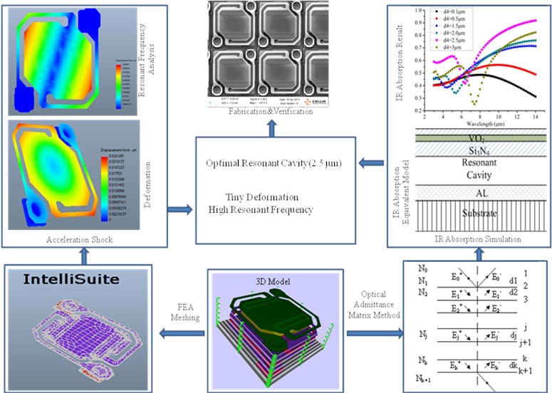
Firstly, three-dimensional (3D) bridge-like structure of a VO2 microbolometer was modeling, as well as an IR absorption equivalent model was established based on the 3D model. IR absorption properties were studied by optical admittance matrix methods and an optimization resonant cavity was given. Then vibration and resonance frequency analysis of microbolometer were finished by the FEA method which should be ensured a good mechanical properties to maintain the resonant cavity of microbolometer as 4 [4].
Fig. 1Simulation flowchart
2.2. Modelling of microbolometer
A 3D model of a VO2 microbolometer shown in Fig. 2 was established. Vibrations and resonant frequency FEA were used to obtain the mechanics and frequency characteristic of the model.
Bridge-like structure, support layer, VO2 resistance layer, passivation layer, absorption layer, electrode, and resonant cavity were established in details by using Intellisuite MEMS software (Fig. 2(a)). 3D mesh diagrams were shown in Fig. 2(b) which the node number of meshing diagrams was 83848. Such an accurate 3D model provides guarantee for an accurate result of FEA.
The types of elements were SOLID95. During FEA, the material properties of 3D mesh Model were defined according to the actual process parameters of their materials. The material properties were listed in Table 1. And then the IR absorption equivalent model was established based on the 3D model was shown in Fig. 3.
The optical admittance matrix model of the IR absorption equivalent model was shown in Fig. 4.
Fig. 2Model of microbolometer
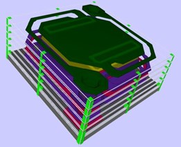
a) 3D model details
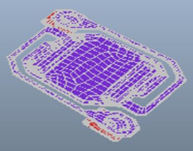
b) 3D mesh diagrams
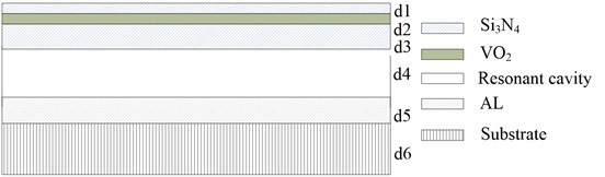
Fig. 3. IR absorption equivalent models (, , , , , were the thickness of Si3N4, VO2, resonant cavity, reflective aluminum and substrate of microbolometer)
Fig. 4The optical admittance matrix model (add and subtract in Ej where the direction of propagation, the dj was thickest, Nj was the plural refractive index of each membrane in microbolometer and given by Nj=nj-ikj, where, nj was the refractive index, kj was extinction coefficient
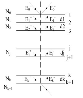
Table 1Microbolometer material properties
Material | Thermal conductivity ( / cm·K) | Thermal capacitance ( / kg·K) | Density ( / cm3) | Resistivity (Ω·Cm) | Young modulus (GPa) | Poisson’s ratio |
Si3N4 | 0.02 | 3.33 | 2.3 | 1×10¹⁵ | 300 | 0.26 |
NiCr | 0.4 | 3.92 | 8.5 | 1×10⁻⁴ | 200 | 0.312 |
VO2 | 0.05 | 5.00 | 4.34 | 1 | 80 | 0.24 |
2.3. IR absorption
The transmittance and the reflectivity could be obtained by calculating the gain matrix of membrane in the infrared wavelength ranged from 8-14 μm and then IR absorption could given by:
Assuming that each membrane were well-proportioned and isotropic, input IR was S-polarized and vertical incidence, the gain matrix of thin film layer was given by:
where, was aphasic thicker and was revised admittance of each membrane respectively. was given by:
where was refractive angle. On the condition of input IR was vertical incidence, the value of was zero. Then, the gain matrix of the entire film series can be expressed by Eq. (4):
where, was the modified admittance. Hence, the combined admittance of multilayer film is . Then the and were expressed by Eq. (5) and Eq. (6) respectively:
where, was the optical admittance of incidence medium. Finally, IR absorption could be obtained by the Eq. (1) via the matlab program. Optical parameters of the IR absorption equivalent model were listed in Table 2.
Table 2Optical parameters of materials
Material | Thickness (μm) | ||
Si3N4 (infrared absorber layer) | 2.1 | 0.01 | 0.03 |
VO2 | 2 | 3 | 0.07 |
Si3N4 (support layer) | 2.1 | 0.01 | 0.3 |
Resonant cavity | 1 | 0 | 2.5 |
Al reflector | 25.4 | 67.3 | 0.5 |
Si substrate | 3.5 | 0 | 5 |
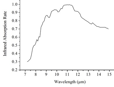
Fig. 5 was the result of IR absorption analysis. It is shown that when the height of resonant cavity was 2.5 μm, the average IR absorption rate had a maximum value as 85.8 % in 8-14 μm.
2.4. Vibrations finite element analysis
Mechanical properties also had an impact effect on the performance of the device. A micro bolometer pixel with a /4 resonant cavity had a maximal infrared absorption rate. The larger or smaller /4 was, the lower infrared absorption rate was. Especially under certain vibrations, the structure of microbolometer should keep small deformation to ensure the resonant cavity was /4. For an IR detector response in 8-14 μm, then was 10 μm [21]. Accelerations vibration shown in Table 3 were loaded on the 3D model at axis, which perpendicular to the bridge-like structure. Mechanical properties of the model were shown in Table 1.
Table 3Acceleration shock FEA parameters
Test equipment | Shock direction | Acceleration shock | Shock pulse width |
Electromagnetic vibration system (D3000-36) | axis | 200 G | 1 ms |
axis | 500 G | 1 ms | |
axis | 1000 G | 1 ms |
Fig. 5Result of IR absorption analysis
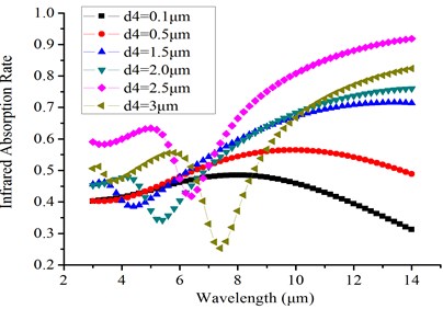
a) IR absorption vs wavelength
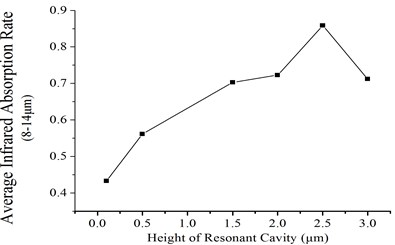
b) Average IR absorption rate vs height of resonant cavity
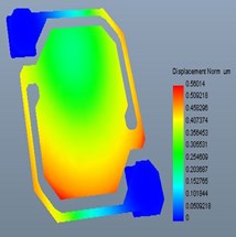
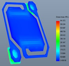
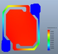
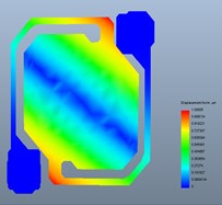
Fig. 6Vibrations FEA results
a) Deformation under 200 G
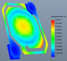
b) Deformation under 500 G
c) Deformation under 1000 G
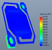
d) Stress distribution under 200 G
e) Stress distribution under 500 G
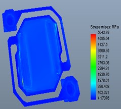
f) Stress distribution under 1000 G
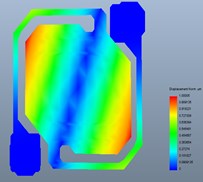
Fig. 6 were the deformation result under acceleration vibration. It can be observed from Fig. 6 that under 200 G and 500 G acceleration, shock at axis, deformation of the model were very small. While the stress of structure under 1000 G acceleration, shock was bigger. It means that under 1000 G acceleration, shock, the structure would be fractured and caused the device failure [18].
Fig. 7 shown the first order modal frequency, the second order modal frequency and, the third order modal frequency was 151215 Hz, 213236 Hz and 318524 Hz respectively. Such a high resonant frequency shown that the device had an excellent mechanical properties under different environment [19].
Fig. 7Results of resonance frequency analysis
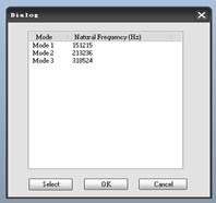
a) Resonant frequency
b) First order modal frequency
c) The second order modal frequency
d) The third order modal frequency
3. Results and discussion
A 320×240 microbolometer with pixels measuring 37×37 μm2 was fabricated according to the design in this study to verify the simulation results. In order to validate properties of the microbolometer in this study, random vibration test was finished according to the test parameters shown in Table 4.
Table 4Random vibration test parameters
Test equipment | Random vibration direction | The intensity of vibration |
Vibration system (M18500 Acceleration METER) | axis | 2 (m/s2) 2/Hz |
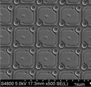
From the SEM of random vibration test shown in Fig. 8, there was little change of internal bridge-like structure and the devices worked properly before and after the test.
Fig. 8SEM of random vibration test on Z axis
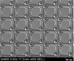
a) Before the vibration
b) After the vibration
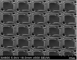
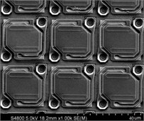
Fig. 9SEM of acceleration, shock test on Z axis
a) 200 G
b) 500 G
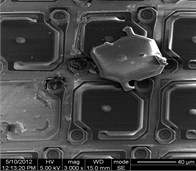
c) 1000 G
d) FIB cross section (1000 G)
Fig. 9(a) and (b) were SEM of microbolometer under 200 G and 500 G acceleration shock. It is shown that the deformation of the model were very small. The resonant cavity was 4 which means high IR absorption for the microbolometer. While under 1000 G acceleration vibration, it can be observed from Fig. 9(c) and (d) that serious deformation and fracture were occurring.
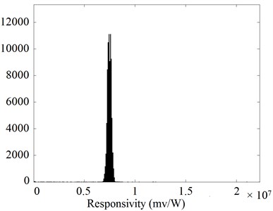
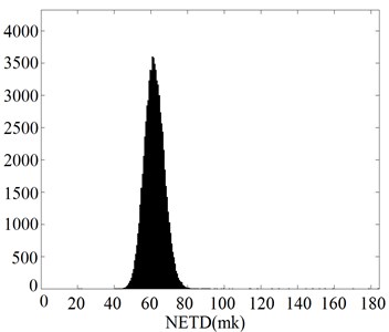
For the excellent mechanical properties, the IR absorption rate of the device was 84.8 % (Fig. 10(a)). High IR absorption result in good responsivity, low noise voltage and NETD which were shown in Figs. 10(b), (c) and (d). Experimental results were listed in Table 5.
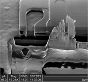
A scanning electron micrograph of the product was shown in Fig. 11(a), (b) was the image captured by the device under 60 Hz.
It is shown the deviation between the measured IR absorption rate was 1.2 %. Experiments versus simulations were as expected. Acceleration shock test results were also in accordance with the vibrations FEA. It suggested that the FEA method was very effective and provided advantages in accuracy.
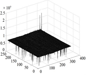
Fig. 10Noise voltage, Responsivity, NETD distributions and IR absorption histograms
a) 3-D Distribution of noise
b) Responsivity histogram
c) NETD histogram
d) IR absorption histogram
Fig. 11Microbolometer as manufactured, and as used
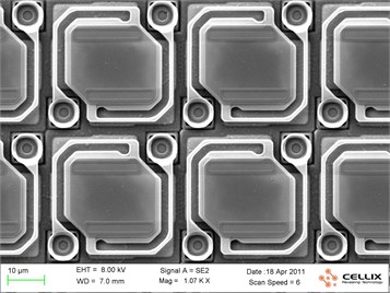
a) Scanning electron microscope (SEM)

b) Image captured (60 Hz)
Table 5Performance of microbolometer (experimental)
Experimental result | Responsivity | NETD | IR absorption rate (8-14 μm) | |
8.61×10⁻⁵ V | 7.42×10⁶ V/W | 61.5 mK | 84.8 % |
4. Conclusions
A novel method for resonant frequency and vibration analysis based on the FEA method was introduced which provide the structure of microbolomer with a good mechanical properties result in a high IR absorption. Finally, a 320×240 IRFPA was fabricated based on this design which had a good mechanical properties leading to excellent performance of the device. Random vibration test and acceleration, shock test was finished and it is showing the experimental results matched simulation results well. This FEA method simulation method offered an efficient ways of microbolometer design and fabrication.
References
-
Chuan Li, et al. Overview of DRS uncooled VOx infrared detector development. Optical Engineering, Vol. 50, Issue 6, 2011, p. 061017.
-
Black S. H., et al. Uncooled detector development at Raytheon. Proceedings of SPIE, Infrared Technology and Applications XXXVII, Vol. 80121A, 2011.
-
Murphy D., et al. 640 x 512 17 μm microbolometer FPA and sensor development. Proceedings of SPIE, Infrared Technology and Applications XXXIII, Vol. 6542, 2007.
-
Kruse P. W., Skatrud D. D. Uncooled Infrared Imaging Arrays and Systems. Academic Press, 1997.
-
Topaloglu N., et al. Modeling of thermal conductance in an uncooled microbolometer pixel. Sensors and Actuators A, Vol 157, Issue 2, 2010, p. 235-245.
-
Seniz E. Kucuk, et al. A detailed analysis for the absorption coefficient of multilevel uncooled infrared detectors. Proceedings of SPIE, Vol. 8012, 2011.
-
Seungoh Han, et al. Parameterized simulation program with integrated circuit emphasis modeling of two-level microbolometer. Journal of Electrical Engineering and Technology, Vol. 6, Issue 2, 2011, p. 270-274.
-
Wang Bt., et al. Finite element model verification for the use of piezoelectric sensor in structural modal analysis. Journal of Mechanics, Vol. 22, Issue 2, 2006, p. 107-114.
-
Saxena Raghvendra Sahai, et al. PSPICE circuit simulation of microbolometer infrared detectors with noise sources. Infrared Physics and Technology, Vol. 55, Issue 6, 2012, p. 527-532.
-
Saxena Raghvendra Sahai, et al. A sub-circuit model of a microbolometer IR detector and its experimental validation. Sensors and Actuators A, Vol. 171, Issue 2, 2011, p. 138-145.
-
Lebedev V., et al. Electrostatically coupled vibration modes in unimorph complementary microcantilevers. Applied Physics Letters, Vol. 100, Issue 12, 2012.
-
Lin Yj., Venna S. V. A novel method for piezoelectric transducers placement for passive vibration control of geometrically non-linear structures. Sensor Review, Vol. 28, Issue 3, 2008, p. 233-241.
-
Goustouridis D., et al. A silicon thermal accelerometer without solid proof mass using porous silicon thermal isolation. IEEE Sensors Journal, Vol. 7, Issue 7, 2007, p. 983-989.
-
Vogl Andreas, et al. Design, process and characterization of a high-performance vibration sensor for wireless condition monitoring. Sensors and Actuators: A. Physical, Vol. 153, Issue 2, 2009, p. 155-161.
-
Wang Yu, et al. A novel micro electric field sensor with X-Y dual axis sensitive differential structure. Sensors and Actuators: A. Physical, Vol. 229, 2015, p. 1-7.
-
Steffen Kurth, et al. Reliability of MEMS devices in shock and vibration overload situations. Proceedings of SPIE, Reliability, Packaging, Testing, and Characterization of MEMS/MOEMS VII, Vol. 6884, Issue 1, 2008, p. 688409-688409-12.
-
Palik E. D. Handbook of Optical Constants of Solids. Academic Press Inc., 1985, p. 394-774.
-
Jinling Wanga, et al. Multiphysics modeling approach for micro electro-thermo-mechanical actuator: failure mechanisms coupled analysis. Microelectronics Reliability, Vol. 55, 2015, p. 771-782.
-
Jámborházi S., et al. Simulating and monitoring the resonant frequency of MEMS for failure detection and prediction. IEEE Conference Publications, Mixed-Signals, Sensors and Systems Test Workshop, 2010, p. 1-5.
-
Hansen K., et al. System-level simulation of an X-ray imager with nonlinear gain and per-pixel digitizer: XPCS case study. Nuclear Instruments and Methods in Physics Research A, Vol. 613, Issue 2, 2010, p. 323-333.
-
Schimert T., et al. Low cost low power un-cooled α Si-based micro infrared camera for unattended ground sensor applications. Proceedings of SPIE, Vol. 3713, 1999, p. 101-111.
About this article
This research was supported by the National Science Foundation of China (Grant No. 61235006, 61421002).
