Abstract
This study is about investigation of design considerations of a MEMS switch that is considered to pull in under electrostatic force generated by a piezoelectric based voltage generator inside the MEMS. Here the energy source to drive the piezoelectric device is vibrations the whole system undergoes. In this study, a new approach is brought to calculate the pull-in voltage easily and effectively under certain assumptions. There are a number of conditions the switch has to meet such as its robustness against environmental vibrations. Some are discussed in brief. Following the design considerations a series of MEMS switches are fabricated and the pull-in voltages are measured in order to compare the true data with calculations and simulations. Numerical results prove the validity of the new approach to calculate the pull-in voltage, and experimental results coincide greatly with the calculations. Several materials are investigated to be used in the design of the cantilever beam and finally a beam structure is proposed that fits best for overall specifications.
1. Introduction
The micro-electro-mechanical systems (MEMS) find more and more application areas every new day due to their advantageous features as small size, low energy consumption, long lifespan and low cost [1]. The micro energy generating devices have become one of the cardinal implementation areas of MEMS structures in recent years. Researches are widely prosecuted especially to supply wireless sensor networks and related communication devices by means of MEMS energy harvesters. Conventional energy sources like batteries do not meet the expectations in wireless networks regarding the size and the need to recharge [2]. Current research studies focus on developing more reliable energy sources to decrease the size of wireless networks and improve the device performances [3]. Thermoelectric, vibration, and radiofrequency power generating systems are being seriously studied, while the preference of the energy harvesting method depends on the application [4].
One of the main components in MEMS-energy source structures is the voltage controlled MEMS switch. This switch serves to connect the circuitry with the voltage generating system. A number of studies are carried out in order to describe the most suitable structure and give related calculations [5, 6]. This study also presents some considerations about the design of MEMS switches to pull in under electrostatic force originally generated by vibrations. In this manner, the natural frequencies of the beam are of high importance that the pull-in action does not happen in consequence of mechanical vibrations, but it is dominantly derived from electrostatic force. Most of the formulas presented in the literature to give the pull-in voltage of the switch result from heavy calculations. They are inherently based upon either the equilibrium of torques or the conservation of energy [7, 8]. This study presents an easy but effective way to calculate the pull-in voltage. Basically some assumptions will be made such as to ignore the stray capacitances of a parallel-plate capacitor, or disregard the curvature of a bending beam. The legitimacy of these assumptions is based upon physical dimensions in practice.
We have been investigating the design considerations of a MEMS switch for quite a period. The results of a previous study are published as a conference paper [9]. This paper carries the aforementioned study an expressive step forward that it contains tips for significant corrections especially about the effect of the base excitation of the beam, presents a new approach to calculate the pull-in voltage and additionally gives true data of a MEMS switch that helps comparison between simulation and realization. We finally propose a structure for the beam that implicates all required features.
2. The role of the MEMS switch
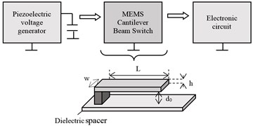
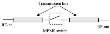
The whole system is considered to contain a micro piezoelectric device as energy harvester (Fig. 1(a)). Under vibrations this device produces charges that are transferred via a rectifier to a capacitor to load it. The produced voltage across the capacitor will help two tasks to be performed. Firstly, it is expected to reach a certain value required by the electronic circuit to supply it. On the other side, this voltage will also be used to generate electrostatic force for pulling in of a MEMS switch in order to provide the connection between the voltage source and the electronic circuit. It’s obvious that the role of a MEMS switch is not restricted with what is explained above. Another application area could be to complete the connection of a transmission line in order to allow the signal reach the output (Fig. 1(b)). In case the voltage drops below the required value, the switch opens (pulls off) and the capacitor keeps on charging.
Fig. 1a) System overview; b) The application of the switch to connect a transmission line
a)
b)
Several investigations are realized to choose the optimum material and structure for the MEMS switch. These are briefly discussed in the following sections.
3. Determination of the pull-in voltage
A voltage applied to two parallel plates causes them to pull each other due to electrostatic force [7]. Consequently the plate separation reduces and at a certain threshold value of the voltage called the pull-in voltage, the plates touch each other. The conventional theory tells that pull-in occurs slightly after the movable plate is deflected about one third of the original separation [1, 7].
For a cantilever beam the calculations can be accomplished as follows:
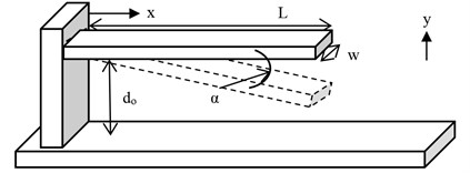
In practice, the separation between the plates () is very small compared with the length of the beam (). Thus, neglecting the curvature, the deflection of the cantilever beam can be demonstrated as in Fig. 2. The differential equation for the deflection of a cantilever beam is given as:
where is the applied torque, the Young’s modulus and the moment of inertia of the cross-sectional area [10]. Since we have a rectangle cross-section, is given as (: thickness of the beam). In case of non-homogenous distribution of the load, Eq. (1) takes the form:
where is the load per unit length.
Fig. 2Cantilever beam
The beam and the bottom electrode form a capacitor of the unit capacitance:
where is the permittivity; and stand for the deflection angle of the beam and the initial gap between the plates, respectively. Here, the stray capacitances are neglected since in practice , . Thus the unit force between the plates is expressed as:
where represents the applied voltage across the capacitor.
Substituting Eq. (4) in Eq. (2), quadruple integrating both sides and arranging the equation to give as a function of yields:
where:
with . Thus, is expressed independent of (for , ). The boundary conditions for the first two integrations are:
while for the last two integrations the conditions follow as:
Since for MEMS cantilever beams , will have very small values so that the curvature of the beam can be neglected and can be assumed to be constant throughout the length , giving , where represents the tip deflection. The maximum of the voltage in the range is called the pull-in voltage .
Chowdhury et al. [7] give the pull-in voltage for the cantilever beam as:
Here, stands for the effective Young’s modulus ( for , : Poisson ratio). They take the stray capacitances into consideration, but they announce the pull-in action for which is valid for parallel-plate case. Eq. 6 is widely used for pull-in voltage calculations; its results also overlap with those of the software COMSOL extensively used for MEMS-design and analysis [9, 11].
Peter M. Osterberg and Stephen D. Senturia give the governing differential equation for the cantilever beam as:
where is the gap between the plates [12].
In practice values for the voltage generated by piezoelectric devices lie in the range of 0.6-1 V [2]. Thus the pull-in voltage should not exceed 1 V. In this study, investigations are carried out for three different materials: Polysilicon, Gold and Aluminum. The approximate value of Young’s modulus and the Poisson ratio for these materials are listed in Table 1.
Table 1Young’s modulus and Poisson ratio for several materials
Material | Young’s modulus () [GPa] | Poisson ratio () |
Polysilicon | 141 | 0.27 |
Aluminum | 70 | 0.33 |
Gold | 79 | 0.44 |
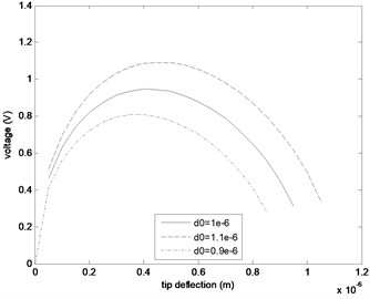
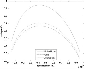
Fig. 3a) Change of V=f(y) with the plate separation d0 (material: Polysilicon), b) V=f(y) curves for different materials (L= 260 μm, w= 50 μm, h= 1 μm and d0= 1 μm)
a)
b)
Fig. 3(a) demonstrates the change of the curve (according to Eq. (5) and for 8.85·10-12 F/m) with the separation between the plates for polysilicon switch of the dimensions 260 μm, 50 μm and 1 μm. The reason for selecting this sample size is that it is suitable for MEMS and gives reasonable values for the voltage applied to the switch [9]. Since the generated voltage is also expected to supply an electronic circuit when the switch closes, its highest possible value is preferable. Regarding this fact, 1 μm fits best for the selected dimensions. We also observe slight shifting of with . Fig. 3(b) shows the curves obtained via Eq. (5) for the selected size and 1 μm for different materials. We observe the pull-in at around 0.4. For the given dimensions, polysilicon is the most advantageous one among the investigated materials since it offers the highest value for .
Table 2 compares the pull-in voltages for polysilicon calculated with Eqs. (5) and (6). The results show satisfactory coincidence. Thus the calculations and assumptions to give Eq. (5) prove their validity.
Table 2Comparison of the calculated values of the pull-in voltage (Material: Polysilicon, dimensions: L= 260 μm, w= 50 μm, h= 1 μm and d0= 1 μm)
Plate separation (μm) | via Eq. (5) (V) | via Eq. (6) (V) |
0.9 | 0.8073 | 0.8125 |
1 | 0.9468 | 0.9508 |
1.1 | 1.0930 | 1.0960 |
4. Considerations about the natural frequencies
In practice the piezoelectric energy harvester undergoes vibrations around 100-250 Hz (i.e. 109 Hz for washing machine, 120 Hz for microwave oven, 240 Hz for refrigerator) [13]. The suitability of the beam conditions that its natural frequencies lie far enough from the environmental oscillations in order to prevent undesired pulling-in. The first natural frequency for a cantilever beam can be derived as:
where represents the mass per length [14]. For the selected sample beam size and 1 μm, the first natural frequencies of the investigated materials are listed in Table 3. It is observed that the natural frequencies for all three materials are far enough from frequencies the piezoelectric device is expected to oscillate, polysilicon showing the best performance.
Table 3First natural frequencies of Polysilicon, Aluminum, and Gold cantilever beams for L= 260 μm, w= 50 μm, h= 1 μm and d0= 1 μm
Beam material | Density (kg/m3) | First natural frequency (kHz) |
Polysilicon | 2330 | 18.590 |
Aluminum | 2700 | 12.166 |
Gold | 19300 | 4.834 |
5. Resistance and pull-out voltage considerations
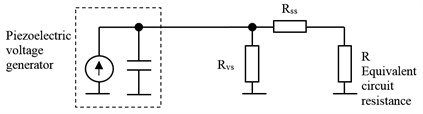
As discussed in Section 2 and demonstrated in Fig. 1(a), the MEMS switch provides the path for the voltage produced by the harvester to supply an electronic circuit. Thus, for the on-resistance (surface resistance ) of the switch a low value is desired so that the voltage drop on the switch itself will be negligible with respect to that across the electronic circuit resulting in low loading effect. On the other side another resistance is effective at the on-position of the switch. Fig. 4(a) illustrates the case the switch is pulled in. In this case certain current flows across the switch (through ) which should be low enough compared with that into the circuit (through ). This can obviously be achieved if the volume resistivity and accordingly the resistance of the switch are high enough.
Since the resistivity for Aluminum and Gold is very low (2.82×10⁻⁸ Ωm for Al, 2.44×10⁻⁸ Ωm for Au), these two materials are not suitable for the whole beam to be made of. On the other hand, the resistivity of 5×1016 cm-3 Phosphorus doped Polysilicon is about 25×103 Ωm which is too high for on-resistance [15]. The best solution is that the cantilever beam will be fabricated using polysilicon covered with a thin layer of conductive material (i.e. Al) for low on-resistance (Fig. 4(b)).
Fig. 4a) Equivalent circuit of the system with the switch in ‘on’ position (Rvs and Rss: Volume resistance and Surface resistance of the switch), b) Concept for the most suitable cantilever beam
a)
b)
For the calculation of the pull-out voltage of cantilever beams of the type we are interested in, no definite model is described in the literature. Since this kind of switch can be observed as a micro relay, the pull-out considerations for those relays can also be applied for our case. Various papers give the information that the pull-out voltage of micro relays is about 80-98 % of the pull-in voltage depending on the materials of the contacts and the structure of the relay [16-18].
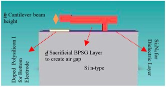
6. Fabrication of polysilicon cantilever beam switch
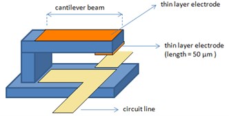
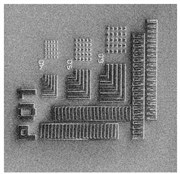
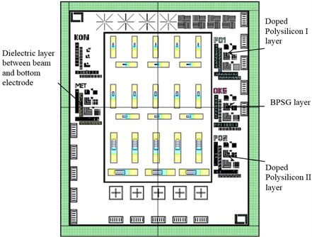
Electrostatically actuated cantilever beam switch is fabricated in YITAL (Semiconductor Technologies Design and Process Research Laboratory) at TUBITAK UEKAE’s clean room (Istanbul-Turkey). In accordance with the considerations about the material of the switch (Fig. 3(b)), Si (1, 0, 0) p-type (Cz) 25 Ω-cm wafers are selected and 5·1015 cm-3 concentrated phosphor doped polysilicon is used for the bottom electrode. Table 4 summarizes the process layers. Scanning Electron Microscope (SEM) image of the mask pattern of the Doped Polysilicon I layer is given in Fig. 5(a). Fig. 5(b) demonstrates the relationship between the beam parts and the layers. The pattern of all layers obtained via L-Edit Software is shown in Fig. 5(c).
Fig. 5a) SEM image of mask pattern of Doped Polysilicon I layer, b) Image of cantilever beam switch (CoventorWare Software), c) The pattern of all layers (L-Edit Software)
a)
c)
b)
Because of some technical constraints the fabricated beam didn’t have the desired dimensions for and . It was fabricated with: 200 μm, 40 μm, 2 μm and 2 μm.
Table 4The process layers of the cantilever beam switch
Material | Thickness | Layer type | Function |
Si | 500 μm | n-type semiconductor | Substrate |
SiO2 | 120 A0 | Dielectric | Decreasing stress between Si3N4 and Si layers |
Si3N4 | 1500 A0 | Dielectric | Dielectric layer between beam and bottom electrode |
Doped Polysilicon I | 3000 A0 | Conductor (n-type) | Bottom electrode |
BPSG | 2 μm | Dielectric (doped SiO2) | Sacrificial Layer for gap between beam and bottom electrode |
Doped Polysilicon II | 2 μm | Conductor (n-type) | Beam |
Aluminum | 2 μm | Conductor | Contact Pads |
7. Measurements and discussions
Due to its fabricated dimensions the beam is not expected to fulfill the pull-in voltage values given in Fig. 3(a) (approx. 1 V) when supplied by a piezoelectric energy harvester. But still it can give idea about the validity of the considerations made for smaller dimensions to achieve low pull-in voltages.
The pull-in voltage of the fabricated beam is calculated as 12.81 V by Eq. (5) and 12.73 V by Eq. (6). But it was measured that the beam pulled in at 12.2 V-12.3 V. The existence of an interval for can be explained with the application speed of the voltage. It is reported experimentally and also explained on mathematical basis that the pull-in occurs for different values of the voltage depending on the speed of the excitation; for step voltage the pull-in appears at around 0.9 [8, 19]. The difference between and can be expounded in various ways such as the errors in dimensions and/or approximations in formulas to model the beam. Furthermore, the Young’s modulus is also very effective in calculations, and its value placed as 141 GPa in the formulas might not be the correct one. Besides the effect of doping, the material properties of silicon depend on orientation relative to the crystal lattice and the value for shows significant change accordingly [20].
On the other side, with the dimensions of 10 μm×50 μm for the Al-contact pad area, the volume resistance of the beam is calculated as 25·103 Ωm×2 μm/500 μm2100 Megohm which is high enough to satisfy the condition for in Fig. 4(a).
8. Conclusion and future work
Some design considerations of a MEMS cantilever beam switch are discussed in this study. The pulling in of the switch is achieved by electrostatic force that is generated by a piezoelectric harvester. Though mainly focused on the calculation of the pull-in voltage, the investigation is also carried out briefly for the natural frequency, resistance and pull-out voltage of the switch. Among the three materials compared (Polysilicon, gold and aluminum), polysilicon is determined as the most suitable one regarding the design considerations taken into account. A simple and effective way to calculate the pull-in voltage is proposed and its validity for practical switch dimensions is proved that the results coincide with those of more complex formulas. Due to some technical constraints, switches of the selected size for 1 V could not be fabricated. Instead, MEMS switches are produced with the dimensions that give higher value for the pull-in voltage. However the consistency between the pull-in voltage measurements and their calculations for these switches shows that the proposed way for the calculations is also applicable on others.
Regarding the considerations taken into account a structure is proposed for the cantilever beam that fits best for overall features.
Further analysis is required for the safety that the beam keeps on working well under the base excitation and limited crush conditions, also proving the considerations about the resonance frequency and related calculations listed in Table 3. Thus, the tip deflection of the beam with non-homogenous load distribution is to be analyzed under the vibration of its base frame. This fact is essentially not a simple modulated vibration of the beam and it requires a very complex analysis, because there is a mutual effect of the electrostatic force and the vibration. The load distribution on the beam related to electrostatic force effects the vibration due to base excitation and vice versa.
References
-
Senturia S. D. Microsystem design. 2nd ed., Kluwer Academic Publishers, Massachusetts, 2001.
-
Kaya T., Koser H., Culurciello E. A low-voltage temperature sensor for micro-power harvesters in silicon-on-sapphire CMOS. Electronics Letters, Vol. 42, Issue 9, 2006.
-
Elfrink R., Kamel T. M., Goedbloed M., Matova S., Hohlfeld D., Van Andel Y., Van Schaijk R. Vibration energy harvesting with aluminum nitride-based piezoelectric devices. Journal of Micromechanics and Microengineering, Vol. 19, Issue 9, 2009.
-
Hudak N. S., Amatucci G. G. Small-scale energy harvesting through thermoelectric, vibration, and radiofrequency power conversion. Journal of Applied Physics, Vol. 103, Issue 10, 2008.
-
Shalaby M. M., Wang Z., et al. Robust design of RF-MEMS cantilever switches using contact physics modeling. IEEE Transactions on Industrial Electronics, Vol. 56, Issue 4, 2009.
-
Peroulis D., Pacheco S. P., et al. Electromechanical considerations in developing low-voltage RF MEMS switches. IEEE Transactions on Microwave Theory and Techniques, Vol. 51, Issue 1, 2003.
-
Chowdhury S., Ahmadi M., MillerW. C. Pull-in voltage calculations for MEMS sensors with cantilevered beams. IEEE-NEWCAS the 3rd International Conference, Québec City, Canada, 2005, p. 143-146.
-
Sattler R., Plötz F., Fattinger G., Wachutka G. Modeling of an electrostatic torsional actuator: demonstrated with an RF MEMS Switch. Sens. Actuators A, Phys., Vol. 97-98, 2002, p. 337-346.
-
Tekin H., İkizoğlu S. Design and simulation of a micro-electro-mechanical switch. International Conference on Electrical and Electronics Engineering, 2009, p. 191-194.
-
Deflection of beams. Chapter 9, 1998, http://ocw.nthu.edu.tw/ocw/upload/8/258/Chapter_9-98.pdf.
-
Comsol Inc. Comsol multiphysics. http://www.comsol.com/products/multiphysics/.
-
Osterberg P. M., Senturia S. D. M-TEST: A test chip for MEMS material property measurement using electrostatically actuated test structures. Journal of Microelectromechanical Systems, Vol. 6, Issue 2, 1997.
-
Wright P., Rabaey J., et al. Industrial and social applications of wireless sensor nets with “energy scavenging” with a case study on “battery-less” tiny-temperature nodes for “smart building applications”. Berkeley Wireless Research Center, Presentation Notes, California, 2002.
-
Irvine T. Application of the newton-raphson method to vibration problems. Vibrationdata Publications, 1999.
-
Plummer J. D., Deal M. D., Griffies P. B. Silicon VLSI technology fundementals, practice and modeling. Printice Hall, 2000.
-
Drake J., Jerman H., Lutze B., Stuber M. An electrostatically actuated micro-relay. The 8th International Conference on Solid-State Sensors and Actuators, Stockholm, Sweden, Vol. 2, 1995, p. 380-383.
-
Grétillat M. A., Grétillat F., De Rooij N. F. Micromechanical relay with electrostatic actuation and metallic contacts. Journal of Micromechanics and Microengineering, Vol. 9, Issue 4, 1999, p. 324-331.
-
Rocha L. A., Cretu E., Wolffenbuttel R. F. Analysis and analytical modeling of static pull-in with application to mems-based voltage reference and process monitoring. Journal of Microelectromechanical Systems, Vol. 13, Issue 2, 2004, p. 342-354.
-
Nielson G. N., Barbastathis G. Dynamic pull-ın of parallel-plate and torsional electrostatic MEMS actuators. Journal of Microelectromechanical Systems, Vol. 15, Issue 4, 2006.
-
Hopcroft M. A., Nix W. D., Kenny T. W. What is the Young’s modulus of silicon? Journal of Microelectromechanical Systems, Vol. 19, Issue 2, 2010.
About this article
